SI2399DS
SI2399DS is P-Channel MOSFET manufactured by Kexin Semiconductor.
Features
- VDS (V) =-20V
- ID =-6 A (VGS =±12V)
- RDS(ON) < 34mΩ (VGS =-10V)
- RDS(ON) < 45mΩ (VGS =-4.5V)
- RDS(ON) < 67mΩ (VGS =-2.5V)
P-Channel MOSFET
SI2399DS (KI2399DS)
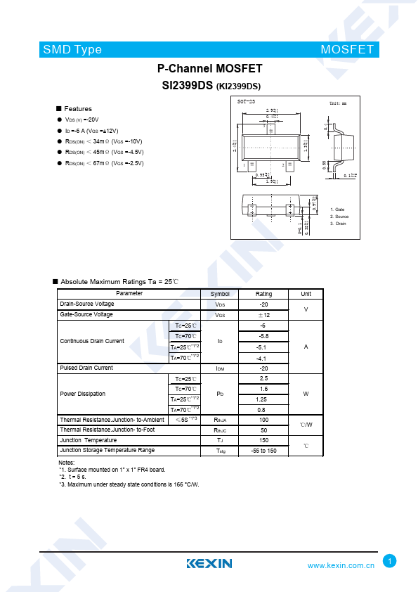
SOT-23
2.9 +0.1 -0.1
0.4 +0.1 -0.1
+0.1 2.4 -0.1
0.95 +0.1 -0.1 1.9 +0.1 -0.1
+0.1 1.3 -0.1
+0.1 0.97 -0.1
MOSFET
Unit: mm
0.1 +0.05 -0.01
1. Gate 2. Source 3. Drain
0-0.1 +0.1 0.38
-0.1
- Absolute Maximum Ratings Ta = 25℃
Parameter
Drain-Source Voltage
Gate-Source Voltage
TC=25℃
Continuous Drain Current
TC=70℃ TA=25℃- 1- 2 TA=70℃- 1- 2
Pulsed Drain Current
TC=25℃
Power Dissipation
Thermal Resistance.Junction- to-Ambient Thermal Resistance.Junction- to-Foot
TC=70℃ TA=25℃- 1- 2 TA=70℃- 1- 2
≤5S
- 1-...