Kexin Electronics WNM2046
N-Channel MOSFET
| Part No. | WNM2046 |
|---|---|
| Datasheet | WNM2046 Download |
| Manufacturer | Kexin Electronics |
| Description | N-Channel MOSFET |
| Buy | Stock & Price |
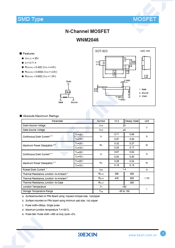
FEATURES
● VDS (V) = 20V● ID = 0.71 A
● RDS(ON) < 0.42Ω (VGS = 4.5V)
● RDS(ON) < 0.500Ω (VGS = 2.5V)
● RDS(ON) < 0.60Ω (VGS = 1.8V) Drain Gate Source 0.00 0.17 0.27 SOT-923 3 0.75 0.85 0.90 1.10 2 1 7º REF. 0.15 Max. 0.05 7º REF. 0.10 0.22 0.35TYP. 0.55 0.65 Uint: mm 0.35 0.43 1. Gate 2. Source 3. Drain
●
ABSOLUTE MAXIMUM RATINGS
Drain-Source Voltage Gate-Source Voltage Parameter Continuous Drain Current a d Maximum Power Dissipation a d Continuous Drain Current b d Maximum Power Dissipation b d Pulsed Drain Current c Thermal Resistance.Junction- to-Ambient a Thermal Resistance.Junction- to-Ambient b Thermal Resistance.Junction- to-Case Junction Temperature Storage Temperature Range TA=25℃ TA=70℃ TA=25℃ TA=70℃ TA=25℃ TA=70℃ TA=25℃ TA=70℃ Symbol VDS VGS ID PD ID PD IDM RthJA RthJA RthJC TJ Tstg a. Surfacemounted on FR4 Board using 1square inchpad size, 1ozcopper b. Surface mounted on FR4 board using minimum pad size, 1oz copper c. Pulse width<380μs, Single pulse d. Maximum junction temperature TJ=150°C. e.