XP162A11
XP162A11 is P-Channel MOSFET manufactured by Kexin Semiconductor.
Features
- VDS (V) =-30V
- ID =-2.5 A (VGS =-10V)
- RDS(ON) < 150mΩ (VGS =-10V)
- RDS(ON) < 280mΩ (VGS =-4.5V)
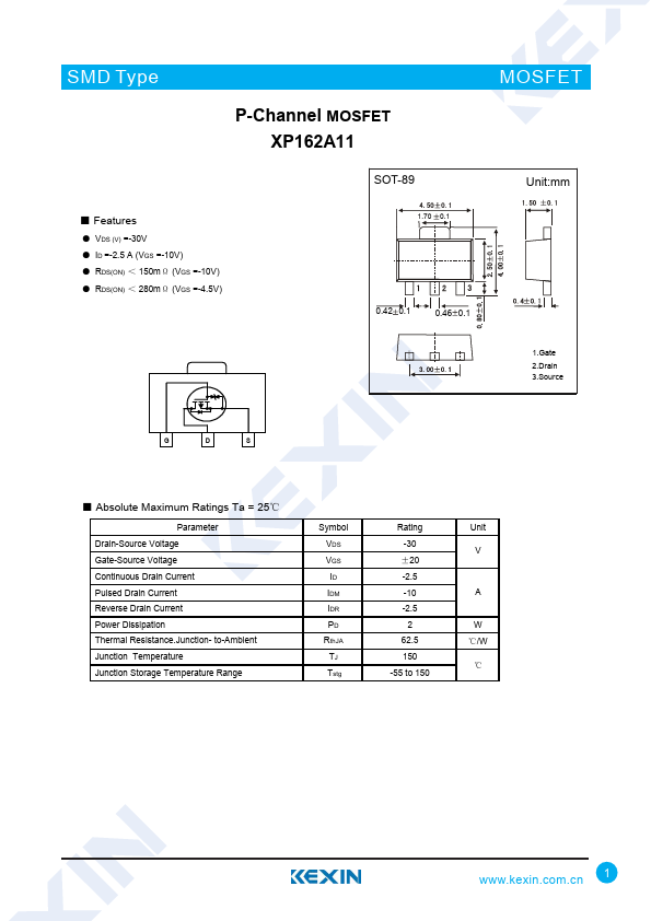
1.70 0.1
0.42 0.1
0.46 0.1
MOSFET
Unit:mm
1.Gate 2.Drain 3.Source
- Absolute Maximum Ratings Ta = 25℃
Parameter Drain-Source Voltage Gate-Source Voltage Continuous Drain Current Pulsed Drain Current Reverse Drain Current Power Dissipation Thermal Resistance.Junction- to-Ambient Junction Temperature Junction Storage Temperature Range
Symbol VDS VGS ID IDM IDR PD Rth JA TJ Tstg
Rating -30 ±20 -2.5 -10 -2.5 2 62.5 150
-55 to 150
Unit V
W ℃/W
℃
.kexin..cn 1
SMD Type
P-Channel MOSFET XP162A11
- Electrical Characteristics Ta = 25℃
Parameter Drain-Source Breakdown Voltage Zero Gate Voltage Drain Current Gate-Body leakage current Gate Cut-off Voltage
Static Drain-Source On-Resistance
Forward Transconductance Input Capacitance Output Capacitance Reverse Transfer Capacitance Turn-On Delay Time Turn-On Rise Time Turn-Off Delay Time Turn-Off Fall Time Diode Forward Voltage
Symbol VDSS IDSS IGSS VGS(off)
RDS(On) g FS Ciss Coss Crss td(on) tr td(off) tf VSD
Test Conditions ID=-250μA, VGS=0V VDS=-30V, VGS=0V VDS=0V, VGS=±20V VGS=-10V, ID=-1m A VGS=-10V, ID=-1.5A VGS=-4.5V, ID=-1.5A VDS=-10V, ID=-1.5A
VGS=0V, VDS=-10V, f=1MHz
VGS=-5V, VDS=-10V, ID=-1.5A
IS=-2.5A,VGS=0V
MOSFET
Min Typ Max...