LS7083NS-14
LS7083NS-14 is QUADRATURE CLOCK CONVERTER manufactured by LSI.
FEATURES
:
- -
- -
- -
- X1 and x4 mode selection Up to 16MHz output clock frequency Programmable output clock pulse width On-chip filtering of inputs for optical or magnetic encoder applications TTL and CMOS patible I/Os +3V to +12V operation (VDD
- VSS) LS7083NS-14 (SOIC)
- See Figure 1.
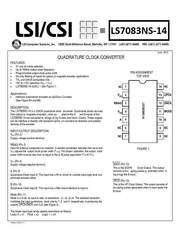
PIN ASSIGNMENT TOP VIEW
Applications:
- Interface incremental encoders to Up/Down Counters (See Figure 6A and 6B)
DESCRIPTION
:
The LS7083NS-14 is a CMOS quadrature clock converter. Quadrature clocks de rived from optical or magnetic encoders, when ap plied to the A and B inputs of the LS7083NS-14 are converted to strings of Up Cl ocks and Down Clocks. These outputs can be interface d directly with standard Up/Do wn counters for direction and position sensing of the encoder.
INPUT/OUTPUT DESCRIPTION
:
VDD (Pin 2) Supply voltage positive terminal. RBIAS (Pin 3) Input for external ponent co nnection. A resistor connected between this inp ut and VSS adjusts the output clock pulse width (T OW). For prope r operation, the output clock pulse width must be less than or equal to the A, B pulse separation (TOW ≤ TPS). VSS (Pin 4) Supply voltage negative terminal. A (Pin 5) Quadrature Clock Input A. This input has a filt er circuit to validate input logic level and eliminate encoder dither. B (Pin 10) Quadrature Clock Input B. This input has a filter circuit identical to input A. Mode (Pin 11) Mode is a 3-sta te input to sele ct resolutions x1, x2, or x4. The selected resolution multiplies the input quadrature clock rate by 1, 2 and 4 respectively; in producing the outputs UPCK/DNCK and CLK (see Figure 2). The Mode input logic levels selects resolutions as follows: Logic 0 = x1 Float = x2 Logic 1 = x4
7083NS-14-062713-1
FIGURE 1.
DNCK (Pin 12) This is the DOWN Clock Output. This output consists of low -going pulses g enerated when A input lags the B input. UPCK (Pin 13) This is the UP Clock Output. This output consists of low-going pulses generated when A input leads the B input.
....