2096VE
Description
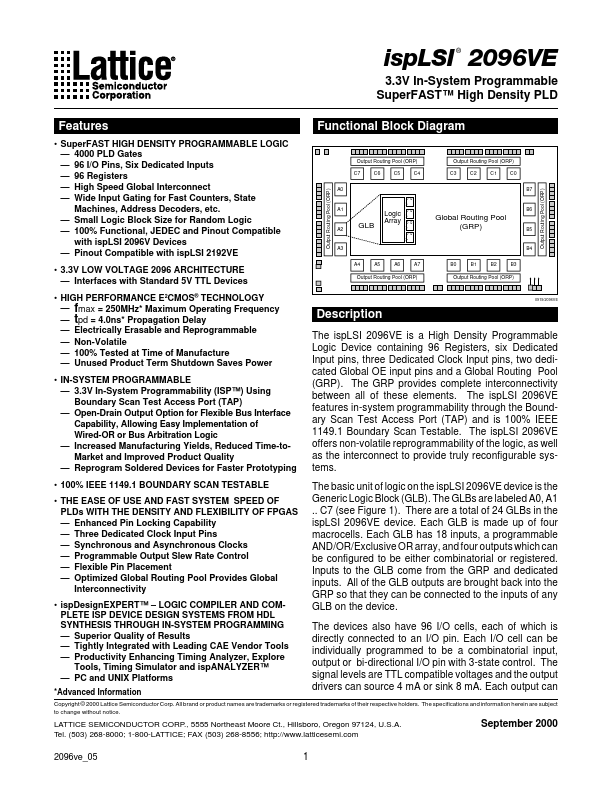
The ispLSI 2096VE is a High Density Programmable Logic Device containing 96 Registers, six Dedicated Input pins, three Dedicated Clock Input pins, two dedicated Global OE input pins and a Global Routing Pool (GRP). The GRP provides complete interconnectivity between all of these elements.
Key Features
- SuperFAST HIGH DENSITY PROGRAMMABLE LOGIC - 4000 PLD Gates - 96 I/O Pins, Six Dedicated Inputs - 96 Registers - High Speed Global Interconnect - Wide Input Gating for Fast Counters, State Machines, Address Decoders, etc. - Small Logic Block Size for Random Logic - 100% Functional, JEDEC and Pinout Compatible with ispLSI 2096V Devices - Pinout Compatible with ispLSI 2192VE
- 3.3V LOW VOLTAGE 2096 ARCHITECTURE - Interfaces with Standard 5V TTL Devices
- HIGH PERFORMANCE E2CMOS® TECHNOLOGY - fmax = 250MHz* Maximum Operating Frequency - tpd = 4.0ns* Propagation Delay - Electrically Erasable and Reprogrammable - Non-Volatile - 100% Tested at Time of Manufacture - Unused Product Term Shutdown Saves Power
- IN-SYSTEM PROGRAMMABLE - 3.3V In-System Programmability (ISP™) Using Boundary Scan Test Access Port (TAP) - Open-Drain Output Option for Flexible Bus Interface Capability, Allowing Easy Implementation of Wired-OR or Bus Arbitration Logic - Increased Manufacturing Yields, Reduced Time-toMarket and Improved Product Quality - Reprogram Soldered Devices for Faster Prototyping
- 100% IEEE 1149.1 BOUNDARY SCAN TESTABLE
- THE EASE OF USE AND FAST SYSTEM SPEED OF PLDs WITH THE DENSITY AND FLEXIBILITY OF FPGAS - Enhanced Pin Locking Capability - Three Dedicated Clock Input Pins - Synchronous and Asynchronous Clocks - Programmable Output Slew Rate Control - Flexible Pin Placement - Optimized Global Routing Pool Provides Global Interconnectivity
- ispDesignEXPERT™ - LOGIC COMPILER AND COMPLETE ISP DEVICE DESIGN SYSTEMS FROM HDL SYNTHESIS THROUGH IN-SYSTEM PROGRAMMING - Superior Quality of Results - Tightly Integrated with Leading CAE Vendor Tools - Productivity Enhancing Timing Analyzer, Explore Tools, Timing Simulator and ispANALYZER™ - PC and UNIX Platforms
- Advanced Information ® Functional Block Diagram Output Routing Pool (ORP) Output Routing Pool (ORP) C7 A0 C6 C5 C4 C3 C2 C1 C0 B7 Output Routing Pool (ORP)
- Q A1 A2 GLB Logic Array
- Q Global Routing Pool (GRP) B5