DESCRIPTION
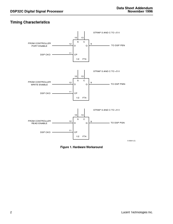
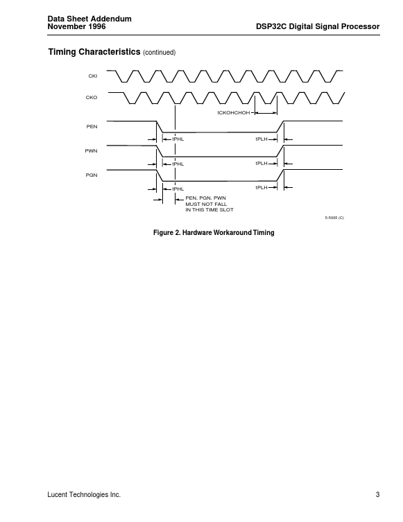
Contents of the PDR register may fail to be transferred to memory during a DMA write operation when the falling edge of PEN or PWN aligns near the trailing edge of the output clock (CKO). If an external device overwrites the PDR, the DMA transaction is not completed. A DMA read transaction may fail if the falling edge of PEN or PGN aligns near the falling edge of CKO. The failure occurs only when the DSP operates at a clock frequency greater than 66 MHz, and CKO is asynchronous with respect to the PEN, PWN, and PGN signals. To eliminate this potential problem, a synchronous clocking scheme is needed. This clocking scheme prevents PEN, PWN and PGN from falling a minimum of 3 ns before the falling edge of CKO. See Figure 2. DSP32C Digital Signal Processor Data Sheet Addendum November 1996 Timing Characteristics STRAP S AND C TO +5 V 10 FROM CONTROLLER PORT ENABLE S 12 D 13 C Q 9 TO DSP PEN DSP CKO 11 CP 1/2 F74 STRAP S AND C TO +5 V 10 FROM CONTROLLER WRITE ENABLE S 12 D 13 C... Lucent Technologies