MX5114D
MX5114D is Single 15A Peak Current Laser Driver manufactured by MAXINMICRO.
FEATURES
- 4V to 20V Single Power Supply
- 15A Peak Current Transient
- 0.4Ω turn on resistance with internal FET
- 5ns (Typical) Propagation Delay
- Matching Delay Time Between Inverting and
Noninverting Inputs
- TTL/CMOS Logic Inputs
- Low Input Capacitance: 2.5p F (Typical)
- - 40°C to 125°C Operating Temperature Range
- 6-Pin DFN2- 2
MX5114D Single 15A Peak Current Laser Driver
APPLICATIONS
Laser driver without external MOSFET
GENERAL INFORMATION
Ordering information
Part Number MX5114D MPQ
Description
DFN2- 2-6L 3000pcs
Package dissipation rating
Package DFN2- 2-6L
RθJA(℃/W) 108.1
Absolute maximum ratings
Parameter VDD to GND IN, INB to GND OUT to GND Junction temperature Storage temperature, Tstg Leading temperature (soldering, 10secs)
ESD Susceptibility HBM
Value -0.3 to 24V -0.3 to 24V -0.3 to VDD+0.3V 150℃ -55 to 150℃
260℃
±2000V
Stresses beyond those listed in Absolute Maximum Ratings may cause permanent damage to the device. Exposure to absolute maximum rating conditions for extended periods may affect reliability. Functional operation of the device at any conditions beyond those indicated in the Remended
Operating Conditions section is not implied.
Remended operating condition
Symbol
Parameter
VDD supply voltage
Junction temperature
Power dissipation
Range 4-20V -40~125℃ 0.73W
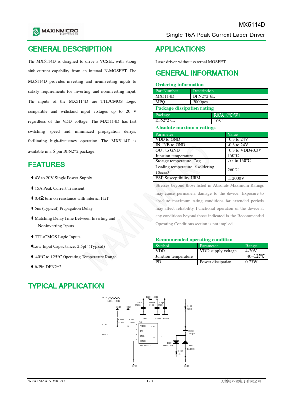
TYPICAL...