BCW68
Features plementary to BCW66, BCW68 is subdivided into three groups F, G and H according to its DC current gain.
Transistor (PNP)
X:Rank
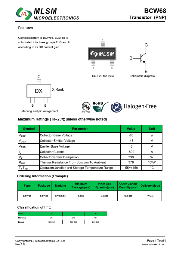
SOT-23 top view
Schematic diagram
Marking and pin assignment
Maximum Ratings (Ta=25℃ unless otherwise noted)
Symbol
VCBO VCEO VEBO IC PC RΘJA TJ,Tstg
Parameter
Collector-Base Voltage Collector-Emitter Voltage Emitter-Base Voltage Collector Current Collector Power Dissipation Thermal Resistance From Junction To Ambient Operation Junction and Storage Temperature Range
Value
-60 -45 -5 -800 330 379 -55~+150
Unit
V V V A W °C/W °C
Ordering Information (Example)
Type
Package
Marking
Minimum Package(pcs)
Inner Box Quantity(pcs)
Outer Carton Quantity(pcs)
Delivery Mode
SOT-23
DF/DG/DH
3,000
45,000
180,000
7"reel
Classification of h FE
Rank Marking Range
F DF 100-250
G DG 160-400
H DH 250-630
Copyright©MLS Microelectronics Co., Ltd Rev 1.0
Page 1 Total 4...