DA221
Features
- Bias circuits
- Protection circuits
SWITCHING DIODE
S1 D2 D1
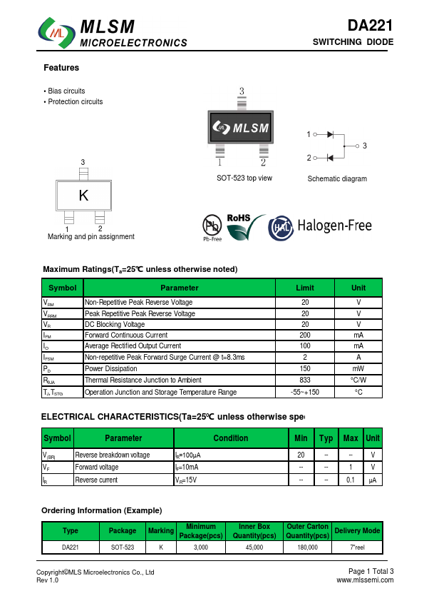
SOT-523 top view
Schematic diagram
Marking and pin assignment
Maximum Ratings(Ta=25℃ unless otherwise noted)
Symbol
Parameter
VRM VRRM VR IFM IO IFSM PD RθJA TJ,TSTG
Non-Repetitive Peak Reverse Voltage Peak Repetitive Peak Reverse Voltage DC Blocking Voltage Forward Continuous Current Average Rectified Output Current Non-repetitive Peak Forward Surge Current @ t=8.3ms Power Dissipation Thermal Resistance Junction to Ambient Operation Junction and Storage Temperature Range
Limit
20 20 20 200 100 2 150 833 -55~+150
Unit
V V V m A m A A m W °C/W °C
ELECTRICAL CHARACTERISTICS(Ta=25℃ unless otherwise spec
Symbol
Parameter
V(BR)
Reverse breakdown voltage
Forward voltage
Reverse current
IR=100μA IF=10m A VR=15V
Condition
Min Typ Max Unit
--
-- V
--
--
1V
--
--
0.1...