IRF7319TRPBF-ML Overview
Key Features
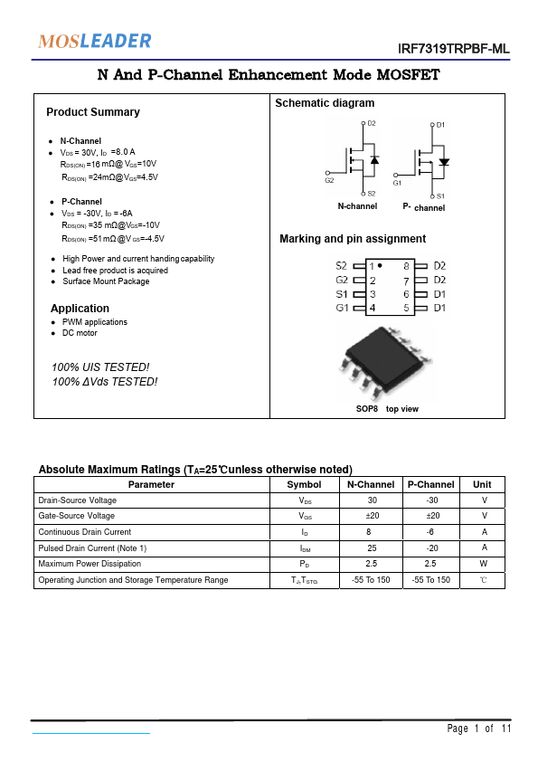
- VDS = 30V, ID =8.0 A
- VDS = -30V, ID = -6A
| Part | IRF7319TRPBF-ML |
|---|---|
| Description | N And P-Channel Enhancement Mode MOSFET |
| Category | MOSFET |
| Manufacturer | MOSLEADER |
| Size | 1.22 MB |
| Part Number | Manufacturer | Description |
|---|---|---|
| IRF7319TR | UMW | MOSFET |
| IRF7319 | International Rectifier | HEXFET Power MOSFET |
| IRF7319PBF | International Rectifier | Power MOSFET |
| IRF7317 | International Rectifier | HEXFET Power MOSFET |
| IRF7314 | International Rectifier | HEXFET Power MOSFET |