Datasheet Summary
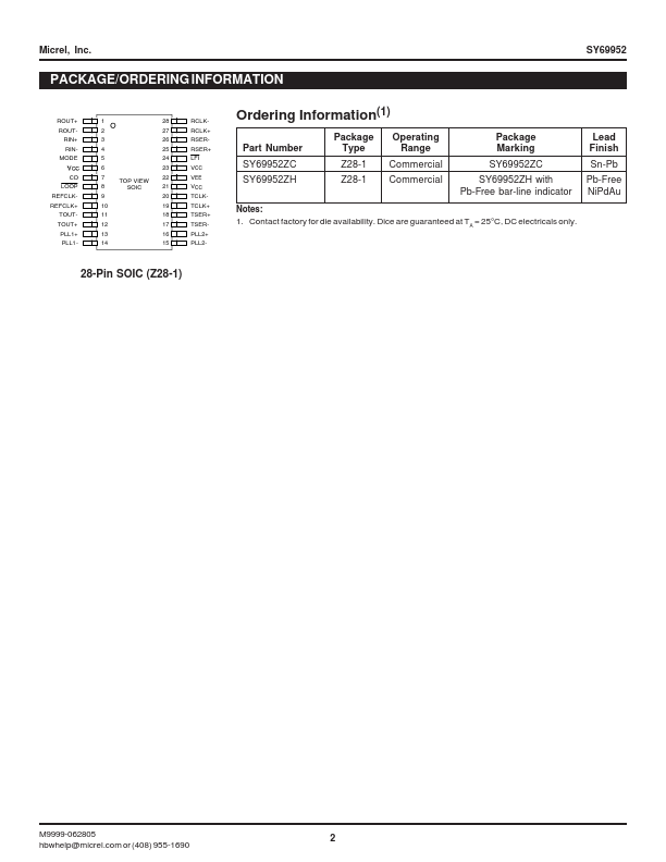
Micrel, Inc.
OC-3/STS-3 CLOCK RECOVERING TRANSCEIVER
Features
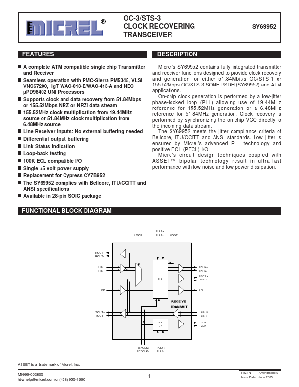
DESCRIPTION
- A plete ATM patible single chip Transmitter and Receiver
- Seamless operation with PMC-Sierra PM5345, VLSI VNS67200, IgT WAC-013-B/WAC-413-A and NEC µPD98402 UNI Processors
- Supports clock and data recovery from 51.84Mbps or 155.52Mbps NRZ or NRZI data stream
- 155.52MHz clock multiplication from 19.44MHz source or 51.84MHz clock multiplication from 6.48MHz source
- Line Receiver Inputs: No external buffering needed
- Differential output buffering
- Link Status Indication
- Loop-back testing
- 100K ECL patible I/O
- Single +5 volt power supply
- Replacement for Cypress CY7B952
- The...