SY89809L
SY89809L is 3.3V 1:9 HIGH-PERFORMANCE / LOW-VOLTAGE BUS CLOCK DRIVER manufactured by Micrel Semiconductor.
Description
The SY89809L is a High-Performance Bus Clock Driver with 9 differential HSTL (High-Speed Transceiver Logic) output pairs. The part is designed for use in low-voltage (3.3V/1.8V) applications, which require a large number of outputs to drive precisely aligned, ultra-low skew signals to their destination. The input is multiplexed from either HSTL or LVPECL (Low-Voltage Positive-Emitter-Coupled Logic) by the CLK_SEL pin. The Output Enable (OE) is synchronous so that the outputs will only be enabled/disabled when they are already in the LOW state. This avoids any chance of generating a runt clock pulse when the device is enabled/disabled as can happen with an asynchronous control.
The SY89809L features low pin-to-pin skew (50ps max.) and low part-to-part skew (200ps max.)- performance previously unachievable in a standard product having such a high number of outputs. The SY89809L is available in a single space saving package, enabling a lower overall cost solution.
Datasheets and support documentation can be found on Micrel’s web site at: .micrel..
Features
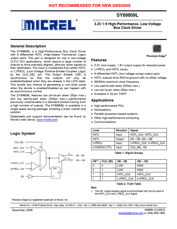
Precision Edge®
- 3.3V core supply, 1.8V output supply for reduced power
- LVPECL and HSTL inputs
- 9 differential HSTL (low-voltage swing) output pairs
- HSTL outputs drive 50Ω-to-ground with no offset voltage
- 500MHz maximum clock frequency
- Low part-to-part skew (200ps max.)
- Low pin-to-pin skew (50ps max.)
- Available in 32-pin TQFP
Applications
- High-performance PCs
- Workstations
- Parallel processor-based systems
- Other high-performance puting
- munications
Logic Symbol
Level HSTL HSTL LVPECL LVCMOS/LVTTL
Direction Input Output Input Input
Signal HSTL_CLK, /HSTL_CLK Q0
- Q8, /Q0
- /Q8 LVPECL_CLK, /LVPECL_CLK CLK_SEL, OE
Table 1. Signal Groups
OE(1) 0 0 1 1
CLK_SEL 0 1 0 1
Q0
- Q8 LOW LOW HSTL_CLK LVPECL_CLK
/Q0
- /Q8 HIGH HIGH /HSTL_CLK /LVPECL_CLK
Table 2. Truth Table
Note: 1. The OE (output enable) signal is synchronized with the low level of the HSTL_CLK and LVPECL_CLK...