FEATURES
s 700MHz min. shift frequency s Extended 100E VEE range of –4.2V to –5.5V s 8 bits wide s Bi-directional s Four selectable modes for full functionality s Asynchronous Master Reset s Fully compatible with industry standard 10KH, 100K ECL levels s Internal 75KΩ input pulldown resistors s Fully compatible with Motorola MC10E/100E141 s Pin-compatible with E241 s Available in 28-pin PLCC package DESCRIPTION
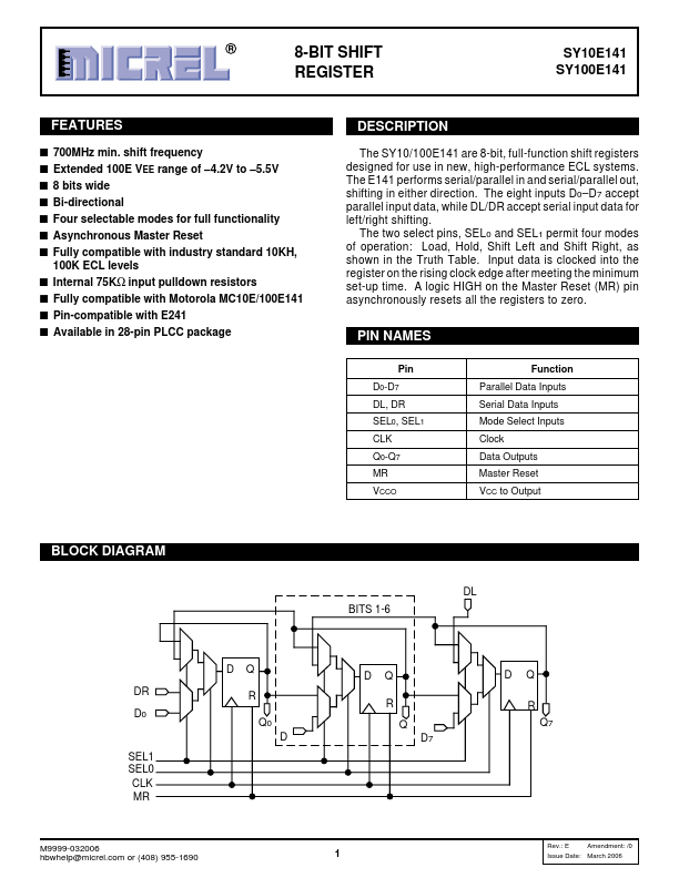
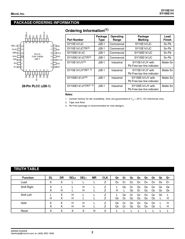
The two select pins, SEL0 and SEL1 permit four modes of operation: Load, Hold, Shift Left and Shift Right, as shown in the Truth Table. Input data is clocked into the register on the rising clock edge after meeting the minimum set-up time. A logic HIGH on the Master Reset (MR) pin asynchronously resets all the registers to zero. PIN NAMES Pin D0-D7 DL, DR SEL0, SEL1 CLK Q0-Q7 MR VCCO Function Parallel Data Inputs Serial Data Inputs Mode Select Inputs Clock Data Outputs Master Reset VCC to Output BLOCK DIAGRAM BITS 1-6 DL DR D0 SEL1 SEL0 CLK MR DQ R Q0 D M9999-032006 hbwhelp@micrel.com or (408) 955-1690 DQ R Q D7 1 DQ R Q7 Rev.: E Amendment: /0 Issue Date: March 2006 Micrel, Inc. Micrel