MT28F800B5 Overview
Key Specifications
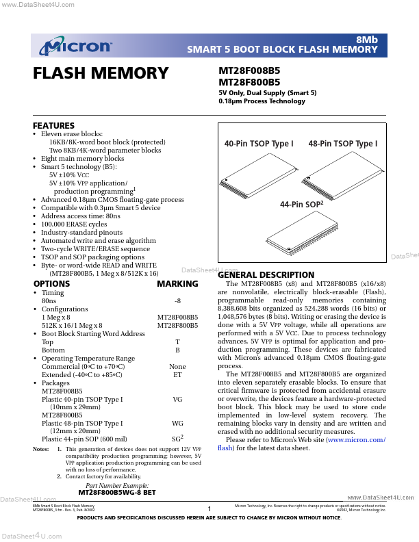
Package: TFSOP
Mount Type: Surface Mount
Pins: 48
Operating Voltage: 5 V
Key Features
- 0.18µm Process Technology
- Eleven erase blocks: 16KB/8K-word boot block (protected) 40-Pin TSOP Type I 48-Pin TSOP Type I Two 8KB/4K-word parameter blocks
- Eight main memory blocks
- Smart 5 technology (B5): 5V ±10% VCC 5V ±10% VPP application/ production programming1
- Advanced 0.18µm CMOS floating-gate process 44-Pin SOP2