MSAER12N50A
MSAER12N50A is N-CHANNEL ENHANCEMENT MODE POWER MOSFET manufactured by Microsemi.
- Part of the MSAFR12N50A comparator family.
- Part of the MSAFR12N50A comparator family.
Features
- -
- -
- -
- Ultrafast rectifier in parallel with the body diode (MSAE type only) Rugged polysilicon gate cell structure Increased Unclamped Inductive Switching (UIS) capability Hermetically sealed, surface mount power package Low package inductance Very low thermal resistance Reverse polarity available upon request
Maximum Ratings @ 25° C (unless otherwise specified)
DESCRIPTION
Drain-to-Source Breakdown Voltage (Gate Shorted to Source)
@ TJ ≥ 25°C
SYMBOL BVDSS BVDGR VGS VGSM ID25 ID100 IDM IAR EAR EAS dv/dt PD Tj Tstg IS ISM θJC
MAX. 500 500 +/-20 +/-30 12 8 48 12 tbd 8 3.5 300 -55 to +150 -55 to +150 12 48 0.4
UNIT Volts Volts Volts Volts Amps Amps Amps m J m J V/ns Watts °C °C Amps Amps °C/W
Drain-to-Gate Breakdown Voltage @ TJ ≥ 25°C, RGS= 1 MΩ Continuous Gate-to-Source Voltage Transient Gate-to-Source Voltage Continuous Drain Current
100°C
Tj= 25°C Tj=
Peak Drain Current, pulse width limited by TJmax Repetitive Avalanche Current Repetitive Avalanche Energy Single Pulse Avalanche Energy Voltage Rate of Change of the Recovery Diode
@ IS ≤ IDM, di/dt ≤ 100 A/µs, VDD ≤ VDSS, TJ ≤ 150°C
Power Dissipation Junction Temperature Range Storage Temperature Range Continuous Source Current (Body Diode) Pulse Source Current (Body Diode) Thermal Resistance, Junction to Case
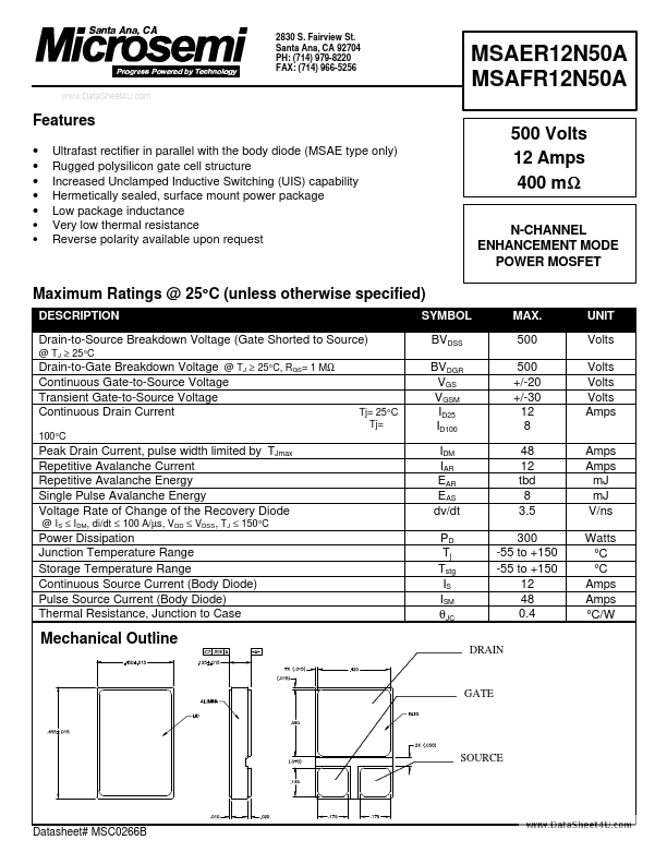
Mechanical Outline
DRAIN
GATE
SOURCE
Datasheet# MSC0266B
MSAER12N50A MSAFR12N50A
..
Electrical Parameters @ 25° C (unless otherwise specified)
DESCRIPTION
Drain-to-Source Breakdown Voltage (Gate Shorted to Source) Temperature Coefficient of the Drain-to-Source Breakdown Voltage Gate Threshold Voltage Gate-to-Source Leakage Current Drain-to-Source Leakage Current (Zero Gate Voltage Drain Current) Static Drain-to-Source On-State Resistance (1)
SYMBOL
BVDSS ∆BVDSS/∆TJ VGS(th) IGSS IDSS RDS(on)
CONDITIONS
VGS = 0 V, I D = 1000 µA
TYP.
UNIT
V V/°C
Forward Transconductance (1) Input Capacitance Output Capacitance Reverse Transfer Capacitance Turn-on Delay Time...