LS3N166
LS3N166 is Amplifier manufactured by Micross.
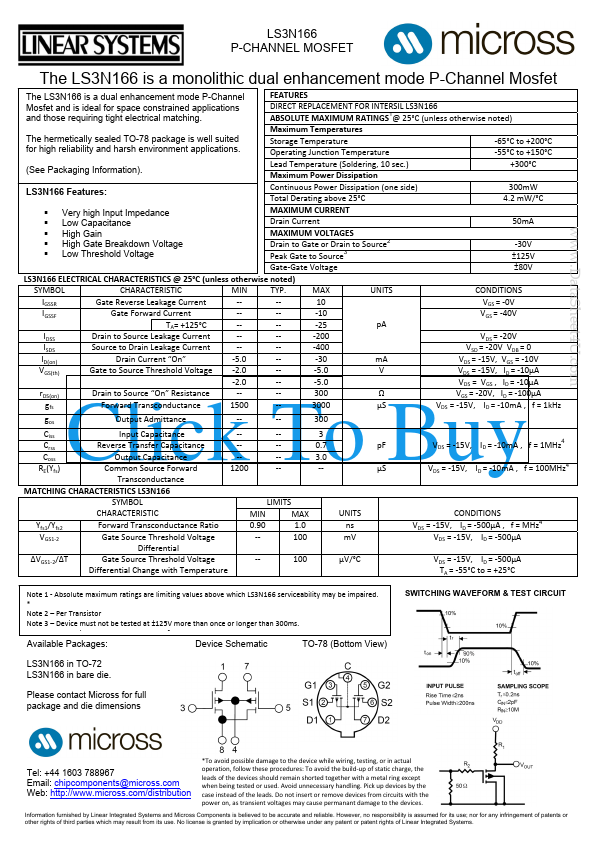
Features
DIRECT REPLACEMENT FOR INTERSIL LS3N166 ABSOLUTE MAXIMUM RATINGS1@ 25°C (unless otherwise noted) Maximum Temperatures The hermetically sealed TO-78 package is well suited Storage Temperature ‐65°C to +200°C for high reliability and harsh environment applications. Operating Junction Temperature ‐55°C to +150°C Lead Temperature (Soldering, 10 sec.) +300°C (See Packaging Information). Maximum Power Dissipation Continuous Power Dissipation (one side) 300m W LS3N166 Features
: Total Derating above 25°C 4.2 m W/°C MAXIMUM CURRENT
- Very high Input Impedance Drain Current 50m A
- Low Capacitance MAXIMUM VOLTAGES
- High Gain
- High Gate Breakdown Voltage Drain to Gate or Drain to Source2 ‐30V
- Low Threshold Voltage Peak Gate to Source3 ±125V Gate‐Gate Voltage ±80V LS3N166 ELECTRICAL CHARACTERISTICS @ 25°C (unless otherwise noted) SYMBOL CHARACTERISTIC MIN TYP. MAX UNITS CONDITIONS IGSSR Gate Reverse Leakage Current ‐‐ ‐‐ 10 VGS = ‐0V IGSSF Gate Forward Current ‐‐ ‐‐ ‐10 VGS = ‐40V p A TA= +125°C ‐‐ ‐‐ ‐25 IDSS Drain to Source Leakage Current ‐‐ ‐‐ ‐200 VDS = ‐20V ISDS Source to Drain Leakage Current ‐‐ ‐‐ ‐400 VSD = ‐20V VDB = 0 ID(on) Drain Current “On” ‐5.0 ‐‐ ‐30 m A VDS = ‐15V, VGS = ‐10V VGS(th) Gate to Source Threshold Voltage ‐2.0 ‐‐ ‐5.0 V VDS = ‐15V, ID = ‐10µA ‐2.0 ‐‐ ‐5.0 VDS = VGS , ID = ‐10µA r DS(on) Drain to Source “On” Resistance ‐‐ ‐‐ 300 Ω VGS = ‐20V, ID = ‐100µA gfs Forward Transconductance 1500 ‐‐ 3000 µS VDS = ‐15V, ID = ‐10m A , f = 1k Hz The LS3N166 is a dual enhancement mode P-Channel Mosfet and is ideal for space constrained applications and those requiring tight electrical matching. gos Ciss Crss Coss RE(Yfs)
..
Input Capacitance ‐‐ ‐‐ 3 p F VDS = ‐15V, ID = ‐10m A , f = 1MHz4 Reverse Transfer Capacitance ‐‐ ‐‐ 0.7 Output Capacitance ‐‐ ‐‐ 3.0 mon Source Forward 1200 ‐‐ ‐‐ µS VDS = ‐15V, ID = ‐10m...