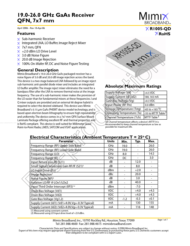
XR1005-QD
Description
Supply Voltage (Vd) Supply Current (Id1,Id2) Gate Bias Voltage (Vg) Input Power (RF Pin) Storage Temperature (Tstg) Operating Temperature (Ta) Channel Temperature (Tch) +4.5 VDC 180, 165 mA +0.3 VDC 0.0 dBm -65 to +165 OC -55 to MTTF Table 3 MTTF Table 3.
Key Features
- The image reject mixer eliminates the need for a bandpass filter after the LNA to remove thermal noise at the image frequency
- The use of a sub-harmonic mixer makes the provision of the LO easier than for fundamental mixers at these frequencies
- I and Q mixer outputs are provided and an external 90 degree hybrid is required to select the desired sideband
- The device es in a 7x7 mm QFN Surface Mount Laminate Package offering excellent RF and thermal properties and is RoHS pliant
- This device is well suited for Millimeter-wave Point-to-Point Radio, LMDS, SAT and VSAT applications


