XR1000
Description
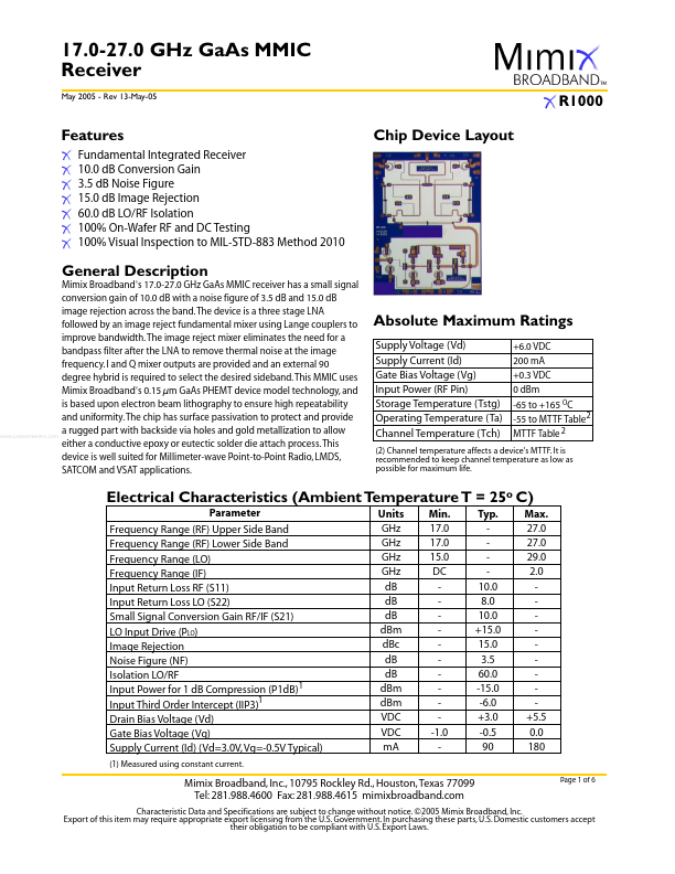
Supply Voltage (Vd) Supply Current (Id) Gate Bias Voltage (Vg) Input Power (RF Pin) Storage Temperature (Tstg) Operating Temperature (Ta) Channel Temperature (Tch) +6.0 VDC 200 mA +0.3 VDC 0 dBm -65 to +165 OC -55 to MTTF Table2 MTTF Table 2 (2) Channel temperature affects a device's MTTF.
Key Features
- The device is a three stage LNA followed by an image reject fundamental mixer using Lange couplers to improve bandwidth
- The image reject mixer eliminates the need for a bandpass filter after the LNA to remove thermal noise at the image frequency
- I and Q mixer outputs are provided and an external 90 degree hybrid is required to select the desired sideband
- This device is well suited for Millimeter-wave Point-to-Point Radio, LMDS, SAT and VSAT applications


