XR1007-QD
XR1007-QD is GaAs Receiver manufactured by Mimix Broadband.
Features
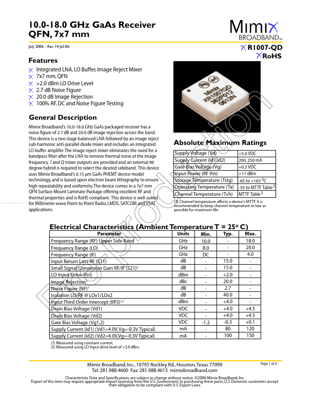
Integrated LNA, LO Buffer, Image Reject Mixer 7x7 mm, QFN +2.0 d Bm LO Drive Level 2.7 d B Noise Figure 20.0 d B Image Rejection 100% RF, DC and Noise Figure Testing
General Description
Mimix Broadband’s 10.0-18.0 GHz Ga As packaged receiver has a noise figure of 2.7 d B and 20.0 d B image rejection across the band. This device is a two stage balanced LNA followed by an image reject sub-harmonic anti-parallel diode mixer and includes an integrated LO buffer amplifer. The image reject mixer eliminates the need for a bandpass filter after the LNA to remove thermal noise at the image frequency. I and Q mixer outputs are provided and an external 90 degree hybrid is required to select the desired sideband. This device uses Mimix Broadband’s 0.15 µm Ga As PHEMT device model technology, and is based upon electron beam lithography to ensure high repeatability and uniformity. The device es in a 7x7 mm QFN Surface Mount Laminate Package offering excellent RF and thermal properties and is Ro HS pliant. This device is well suited for Millimeter-wave Point-to-Point Radio, LMDS, SAT and VSAT applications.
Absolute Maximum Ratings
Supply Voltage (Vd) Supply Current (Id1,Id2) Gate Bias Voltage (Vg) Input Power (RF Pin) Storage Temperature (Tstg) Operating Temperature (Ta) Channel Temperature (Tch)
+5.0 VDC 200, 250 m A +0.3 VDC +17 d Bm -65 to +165 OC -55 to MTTF Table 3 MTTF Table 3
..
(3) Channel temperature affects a device's MTTF. It is remended to keep channel temperature as low as possible for maximum life.
Electrical Characteristics (Ambient Temperature T = 25o C)
Parameter Frequency Range (RF) Upper Side Band Frequency Range (LO) Frequency Range (IF) Input Return Loss RF (S11) Small Signal Conversion Gain RF/IF (S21)2 LO Input Drive (PLO) Image Rejection2 Noise Figure (NF)2 Isolation LO/RF @ LOx1/LOx2 Input Third Order Intercept (IIP3)1,2 Drain Bias Voltage (Vd1) Drain Bias Voltage (Vd2) Gate Bias Voltage (Vg1,2) Supply Current (Id1) (Vd1=4.0V, Vg=-0.3V Typical) Supply...