Datasheet4U Logo Datasheet4U.com

M5M5T5672TG-20 - 18874368-BIT(262144-WORD BY 72-BIT) NETWORK SRAM

Description

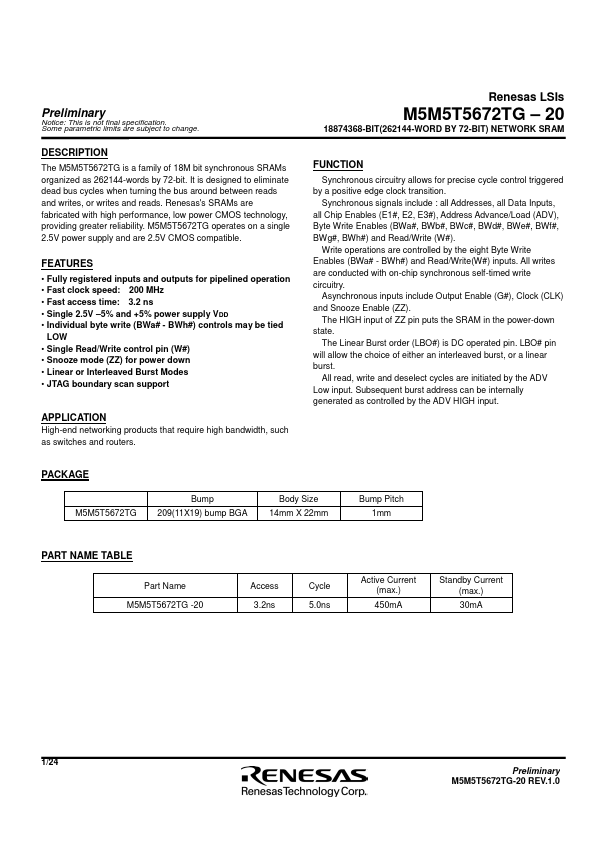
The M5M5T5672TG is a family of 18M bit synchronous SRAMs organized as 262144-words by 72-bit.

It is designed to eliminate dead bus cycles when turning the bus around between reads and writes, or writes and reads.

Features

  • Fully registered inputs and outputs for pipelined operation.
  • Fast clock speed: 200 MHz.
  • Fast access time: 3.2 ns.
  • Single 2.5V.
  • 5% and +5% power supply VDD.
  • Individual byte write (BWa# - BWh#) controls may be tied LOW.
  • Single Read/Write control pin (W#).
  • Snooze mode (ZZ) for power down.
  • Linear or Interleaved Burst Modes.
  • JTAG boundary scan support.

📥 Download Datasheet

Datasheet preview – M5M5T5672TG-20

Datasheet Details

Part number M5M5T5672TG-20
Manufacturer Mitsubishi
File Size 370.31 KB
Description 18874368-BIT(262144-WORD BY 72-BIT) NETWORK SRAM
Datasheet download datasheet M5M5T5672TG-20 Datasheet
Additional preview pages of the M5M5T5672TG-20 datasheet.
Other Datasheets by Mitsubishi

Full PDF Text Transcription

Click to expand full text
Preliminary Notice: This is not final specification. Some parametric limits are subject to change. DESCRIPTION The M5M5T5672TG is a family of 18M bit synchronous SRAMs organized as 262144-words by 72-bit. It is designed to eliminate dead bus cycles when turning the bus around between reads and writes, or writes and reads. Renesas's SRAMs are fabricated with high performance, low power CMOS technology, providing greater reliability. M5M5T5672TG operates on a single 2.5V power supply and are 2.5V CMOS compatible. FEATURES • Fully registered inputs and outputs for pipelined operation • Fast clock speed: 200 MHz • Fast access time: 3.2 ns • Single 2.
Published: |