BFR30LT1
Overview
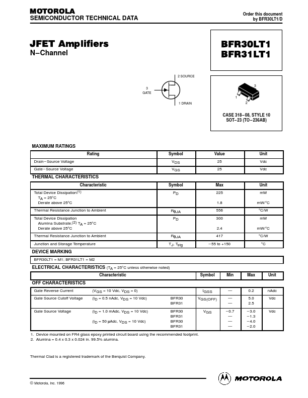
MOTOROLA SEMICONDUCTOR TECHNICAL DATA Order this document by BFR30LT1/D JFET Amplifiers N–Channel 2 SOURCE 3 GATE BFR30LT1 BFR31LT1 3 1 1 DRAIN 2 CASE 318 – 08, STYLE 10 SOT– 23 (TO – 236AB) M...
| Part | BFR30LT1 |
|---|---|
| Description | JFET Amplifiers |
| Manufacturer | Motorola Semiconductor |
| Size | 136.66 KB |
MOTOROLA SEMICONDUCTOR TECHNICAL DATA Order this document by BFR30LT1/D JFET Amplifiers N–Channel 2 SOURCE 3 GATE BFR30LT1 BFR31LT1 3 1 1 DRAIN 2 CASE 318 – 08, STYLE 10 SOT– 23 (TO – 236AB) M...
| Part Number | Manufacturer | Description |
|---|---|---|
| BFR30LT1 | onsemi | JFET Amplifiers |
| BFR30 | Motorola Semiconductor | JFET |
| BFR30 | NXP Semiconductors | N-channel field-effect transistors |