BFR30
Overview
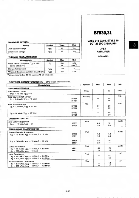
BFR30,31 MAXIMUM RATINGS Rating Drain-Source Voltage Gate-Source Voltage Symbol VDS vgs THERMAL CHARACTERISTICS Characteristic Symbol "Total Device Dissipation, T^ = 25°C Derate above 25°C PD ...
| Part | BFR30 |
|---|---|
| Description | JFET |
| Manufacturer | Motorola Semiconductor |
| Size | 30.97 KB |
BFR30,31 MAXIMUM RATINGS Rating Drain-Source Voltage Gate-Source Voltage Symbol VDS vgs THERMAL CHARACTERISTICS Characteristic Symbol "Total Device Dissipation, T^ = 25°C Derate above 25°C PD ...
| Part Number | Manufacturer | Description |
|---|---|---|
| BFR30LT1 | onsemi | JFET Amplifiers |
| BFR30 | NXP Semiconductors | N-channel field-effect transistors |
| BFR360F | Infineon | Low Noise Silicon Bipolar RF Transistor |
| BFR380T | Infineon | NPN Silicon RF Transistor |
| BFR31LT1 | onsemi | JFET Amplifiers |