Motorola BUX41
NPN Transistor
| Part No. | BUX41 |
|---|---|
| Datasheet | BUX41 Download |
| Manufacturer |  Motorola |
| Description | NPN Transistor |
| Buy | Stock & Price |
MAXIMUM RATINGS
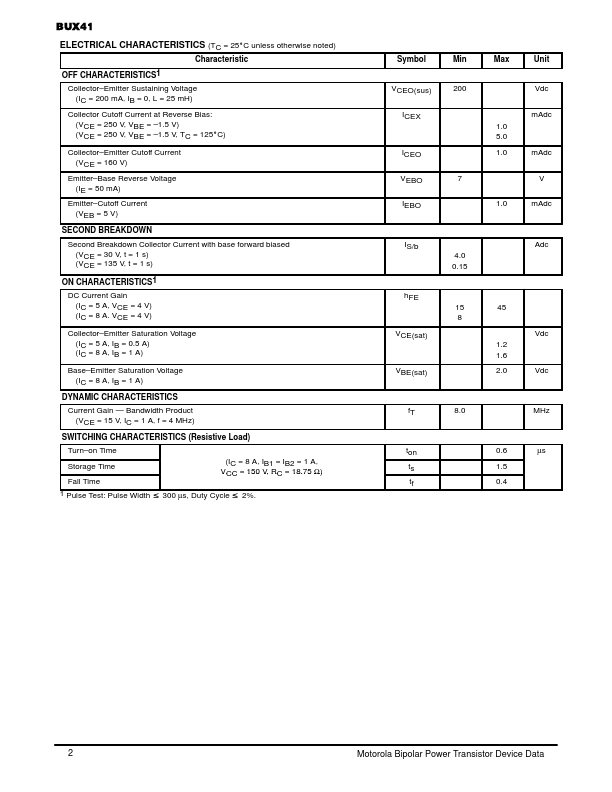
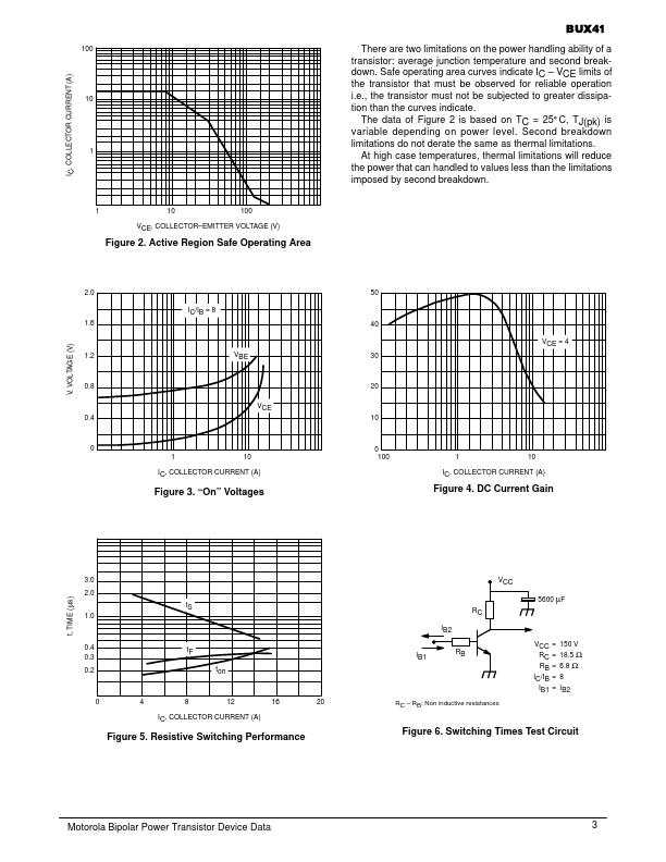
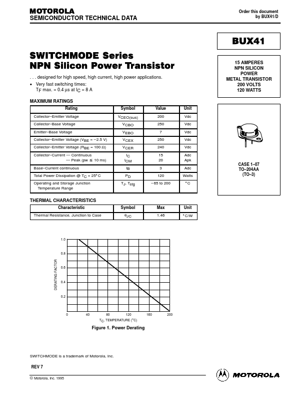
Rating Symbol Value 200 250 7 Unit Vdc Vdc Vdc Vdc Vdc Adc Apk Adc Collector–Emitter Voltage Collector–Base Voltage Emitter–Base Voltage VCEO(sus) VCBO VEBO VCEX Collector–Emitter Voltage (VBE = – 2.5 V) Collector–Emitter Voltage (RBE = 100 Ω) 250 240 15 20 3 VCER IC ICM IB Collector–Current — Continuous Collector–Current — Peak (pw 10 ms) Base–Current continuous Total Power Dissipation @ TC = 25_C Operating and Storage Junction Temperature Range PD 120 Watts TJ, Tstg – 65 to 200 . . . designed for high speed, high current, high power applications. CASE 1–07 TO–204AA (TO–3) _C THERMAL CHARACTERISTICS Characteristic Symbol θJC Max Unit Thermal Resistance, Junction to Case 1.46 _C/W 1.0 0.8 DERATING FACTOR 0.6 0.4 0.2 0 40 80 120 TC, TEMPERATURE (°C) 160 200 Figure 1. Power Derating SWITCHMODE is a trademark of Motorola, Inc. REV 7 © Motorola, Inc. 1995 Motorola Bipolar Power Transistor Device Data 1 BUX41 ÎÎÎÎÎÎÎÎÎÎÎÎÎÎÎÎÎÎÎÎÎÎÎ ÎÎÎÎ ÎÎÎÎ ÎÎÎÎ ÎÎÎ ÎÎÎÎÎÎÎÎÎÎÎÎÎÎÎÎÎÎÎÎÎÎÎ...