MC100ELT25
features
. The VBB output allows the ELT25 to also be used in a single-ended input mode. In this mode the VBB output is tied to the IN input for a non-inverting buffer or the IN input for an inverting buffer. If used the VBB pin should be bypassed to ground via a 0.01µF capacitor. The ELT25 is available in both ECL standards: the 10ELT is patible with MECL 10H logic levels while the 100ELT is patible with ECL 100K logic levels.
MC10ELT25 MC100ELT25
8 1
- -
- -
- 2.6ns Typical Propagation Delay Differential ECL Inputs Small Outline SOIC Package 24m A TTL Outputs Flow Through Pinouts
D SUFFIX PLASTIC SOIC PACKAGE CASE 751-05
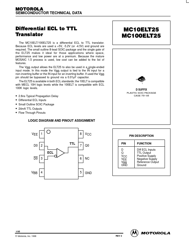
LOGIC DIAGRAM AND PINOUT ASSIGNMENT
VEE 1 TTL ECL D0 3
PIN D Q VCC VEE VBB GND
PIN DESCRIPTION
FUNCTION Diff ECL Inputs TTL Output Positive Supply Negative Supply Reference Output Ground
D0
Q0
1/95
© Motorola, Inc. 1996
3- 1
REV 2
MC10ELT25 MC100ELT25
MAXIMUM RATINGS-
Symbol VCC VEE VIN IOUT TA TSTG Parameter DC...