Datasheet Summary
MOTOROLA
SEMICONDUCTOR TECHNICAL DATA
Order this document by MCM69Q618/D
Advance Information
64K x 18 Bit Synchronous Separate I/O Fast SRAM
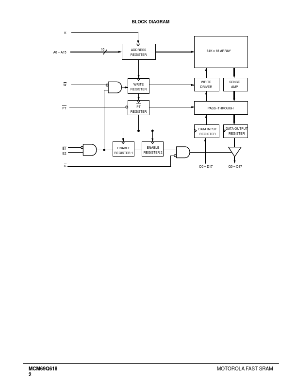
The Motorola MCM69Q618 is a 1 Megabit static random access memory, organized as 64K words of 18 bits. It Features separate data input and data output buffers and incorporates input and output registers on board with high speed SRAM. The MCM69Q618 allows the user to perform transparent write and data pass through. Two data bus ports are provided
- a data input (D) and a data output (Q) port. The synchronous design allows for precise cycle control with the use of an external single clock (K). Address port, data input (D0
- D17), data...