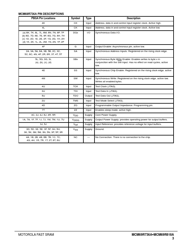
Datasheet4U Logo Datasheet4U.com

MCM69R818A - Memory Products

General Description

PBGA Pin Locations 4K 4L (a) 6K, 7K, 6L, 7L, 6M, 6N, 7N, 6P, 7P (b) 6D, 7D, 6E, 7E, 6F, 6G, 7G, 6H, 7H (c) 1D, 2D, 1E, 2E, 2F, 1G, 2G, 1H, 2H (d) 1K, 2K, 1L, 2L, 2M, 1N, 2N, 1P, 2P 4F 2A, 3A, 5A, 6A, 3B, 5B, 2C, 3C, 5C, 6C, 4N, 4P, 2R, 6R, 3T, 4T, 5T 5L, 5G, 3G, 3L (a), (b), (c), (d) 4E 4M 4U 3U 5U

Key Features

  • >.
  • 35 High.
  • Z High.
  • Z High.
  • Z High.
  • Z Mode Read Cycle All Bytes Write Cycle 1st Byte Write Cycle 2nd Byte Write Cycle 3rd Byte Write Cycle 4th Byte Write Cycle All Bytes Abort Write Cycle Deselect Cycle Deselect Cycle Sleep Mode.

📥 Download Datasheet

Full PDF Text Transcription (Reference)

The following content is an automatically extracted verbatim text from the original manufacturer datasheet and is provided for reference purposes only.

View original datasheet text
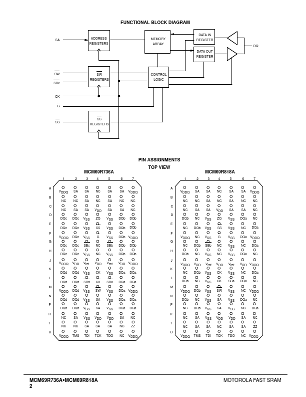
MOTOROLA SEMICONDUCTOR TECHNICAL DATA Order this document by MCM69R736A/D Advance Information 4M Late Write HSTL The MCM69R736A/818A is a 4 megabit synchronous late write fast static RAM designed to provide high performance in secondary cache and ATM switch, Telecom, and other high speed memory applications. The MCM69R818A organized as 256K words by 18 bits, and the MCM69R736A organized as 128K words by 36 bits wide are fabricated in Motorola’s high performance silicon gate BiCMOS technology. The differential CK clock inputs control the timing of read/write operations of the RAM. At the rising edge of the CK clock all addresses, write enables, and synchronous selects are registered.