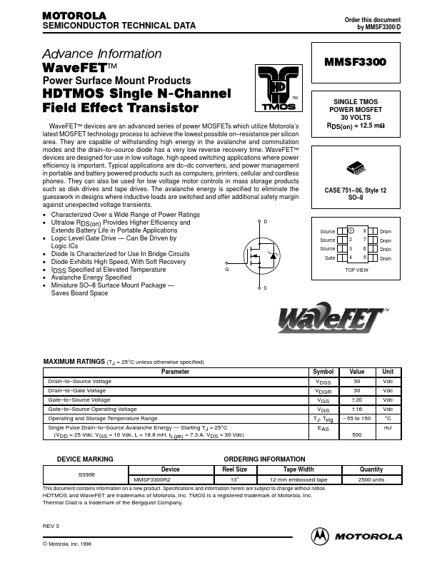
Datasheet4U Logo Datasheet4U.com

MMSF3300 - SINGLE TMOS POWER MOSFET

Key Features

  • re VGG = the gate drive voltage, which varies from zero to VGG RG = the gate drive resistance and Q2 and VGSP are read from the gate charge curve. During the turn.
  • on and turn.
  • off delay times, gate current is not constant. The simplest calculation uses appropriate values from the capacitance curves in a standard equation for voltage change in an RC network. The equations are: td(on) = RG Ciss In [VGG/(VGG.
  • VGSP)] td(off) = RG Ciss In (VGG/VGSP) The capacitance (Ciss) is r.

📥 Download Datasheet

Full PDF Text Transcription (Reference)

The following content is an automatically extracted verbatim text from the original manufacturer datasheet and is provided for reference purposes only.

View original datasheet text
MOTOROLA SEMICONDUCTOR TECHNICAL DATA Order this document by MMSF3300/D Advance Information WaveFET™ Power Surface Mount Products MMSF3300 ™ HDTMOS Single N-Channel Field Effect Transistor WaveFET™ devices are an advanced series of power MOSFETs which utilize Motorola’s latest MOSFET technology process to achieve the lowest possible on–resistance per silicon area. They are capable of withstanding high energy in the avalanche and commutation modes and the drain–to–source diode has a very low reverse recovery time. WaveFET™ devices are designed for use in low voltage, high speed switching applications where power efficiency is important.