MTD3055V Overview
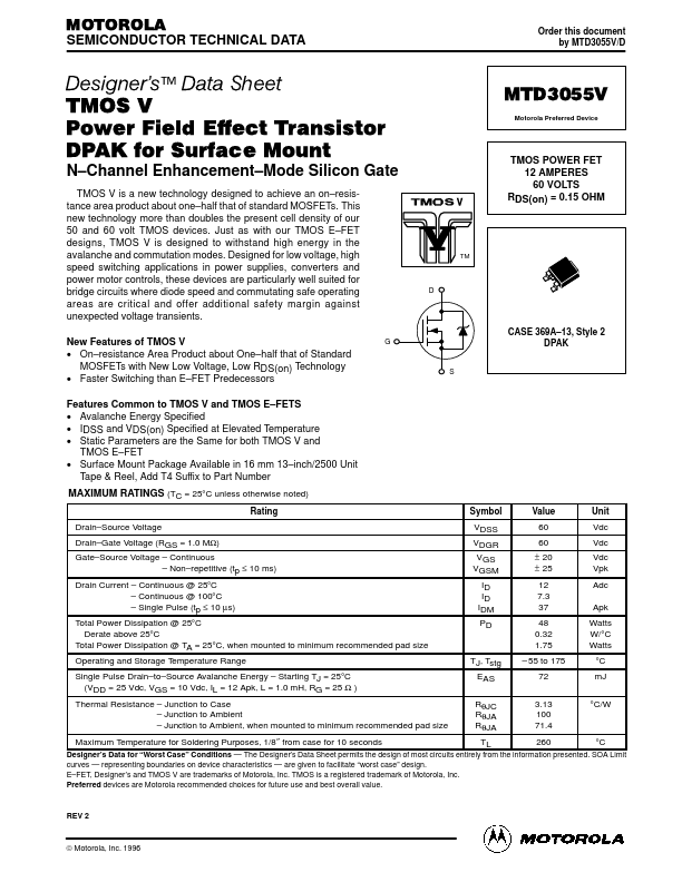
MOTOROLA Designer's SEMICONDUCTOR TECHNICAL DATA Order this document by MTD3055V/D TMOS V Power Field Effect Transistor DPAK for Surface Mount TMOS V is a new technology designed to achieve an on resistance area product about one half that of standard MOSFETs. This new technology more than doubles the present cell density of our 50 and 60 volt TMOS devices. Just as with our TMOS E FET designs, TMOS V is designed to...
MTD3055V Key Features
- On-resistance Area Product about One-half that of Standard MOSFETs with New Low Voltage, Low RDS(on) Technology
- Faster Switching than E-FET Predecessors Features mon to TMOS V and TMOS E-FETS
- Avalanche Energy Specified
- IDSS and VDS(on) Specified at Elevated Temperature
- Static Parameters are the Same for both TMOS V and TMOS E-FET
- Surface Mount Package Available in 16 mm 13-inch/2500 Unit Tape & Reel, Add T4 Suffix to Part Number MAXIMUM RATINGS (TC
- Continuous Gate-Source Voltage
- Non-repetitive (tp ≤ 10 ms) Drain Current
- Continuous @ 25°C Drain Current
- Continuous @ 100°C Drain Current
MTD3055V Applications
- On-resistance Area Product about One-half that of Standard MOSFETs with New Low Voltage, Low RDS(on) Technology
- Faster Switching than E-FET Predecessors Features mon to TMOS V and TMOS E-FETS