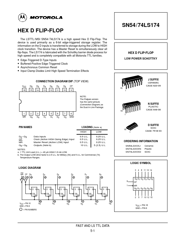
Download the SN74LS174 datasheet PDF.
This datasheet also covers the SN74LS174D variant, as both devices belong to the same hex d flip-flop family and are provided as variant models within a single manufacturer datasheet.
Full PDF Text Transcription for SN74LS174 (Reference)
Note: Below is a high-fidelity text extraction (approx. 800 characters) for
SN74LS174. For precise diagrams, and layout, please refer to the original PDF.
HEX D FLIP-FLOP The LSTTL / MSI SN54 / 74LS174 is a high speed Hex D Flip-Flop. The device is used primarily as a 6-bit edge-triggered storage register. The information o...
View more extracted text
rimarily as a 6-bit edge-triggered storage register. The information on the D inputs is transferred to storage during the LOW to HIGH clock transition. The device has a Master Reset to simultaneously clear all flip-flops. The LS174 is fabricated with the Schottky barrier diode process for high speed and is completely compatible with all Motorola TTL families. • Edge-Triggered D-Type Inputs • Buffered-Positive Edge-Triggered Clock • Asynchronous Common Reset • Input Clamp Diodes Limit High Speed Termination Effects CONNECTION DIAGRAM DIP (TOP VIEW) VCC Q5 D5 D4 Q4 D3 Q3 CP 16 15 14 13 12 11 10 9 NOTE: The Flatpak version ha