NCE Power Semiconductor NCE01P13
The NCE01P13 uses advanced trench technology and design to provide excellent RDS(ON) with low gate charge. It can be used in a wide variety of applications.| Part No. | NCE01P13 |
|---|---|
| Datasheet | NCE01P13 Download |
| Manufacturer |  NCE Power Semiconductor |
| Description | P-Channel Enhancement Mode Power MOSFET |
| Buy | Stock & Price |
DESCRIPTION
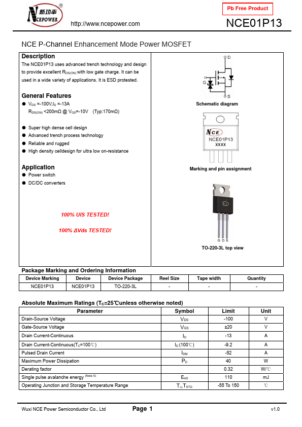
It can be used in a wide variety of applications. It is ESD protested.GENERAL FEATURES
● VDS =-100V,ID =-13A RDS(ON) <200mΩ @ VGS=-10V (Typ:170mΩ)● Super high dense cell design
● Advanced trench process technology
● Reliable and rugged
● High density celldesign for ultra low on-resistance Schematic diagram Application
● Power switch
● DC/DC converters Marking and pin assignment 100% UIS TESTED! 100% ∆Vds TESTED! TO-220-3L top view Package Marking and Ordering Information Device Marking Device Device Package NCE01P13 NCE01P13 TO-220-3L Reel Size - Tape width - Quantity -
ABSOLUTE MAXIMUM RATINGS
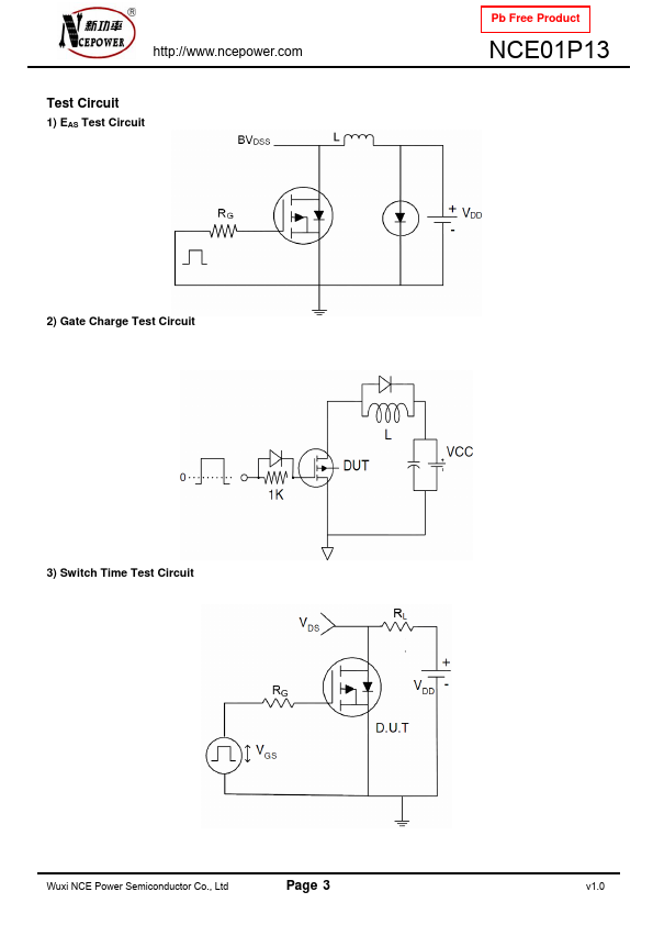
(TC=25℃unless otherwise noted) Parameter Symbol Drain-Source Voltage VDS Gate-Source Voltage VGS Drain Current-Continuous ID Drain Current-Continuous(TC=100℃) ID (100℃) Pulsed Drain Current Maximum Power Dissipation IDM PD Derating factor Single pulse avalanche energy (Note 5) EAS Operating Junction and Storage Temperature Range TJ,TSTG Limit -100 ±20 -13 -9.2 -52 40 0.32 110 -55 T...