Datasheet4U Logo Datasheet4U.com

NCEP023N10LL - N-Channel Super Trench II Power MOSFET

General Description

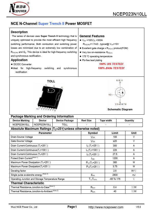
The series of devices uses Super Trench II technology that is uniquely optimized to provide the most efficient high frequency switching performance.

Both conduction and switching power losses are minimized due to an extremely low combination of RDS(ON) and Qg.

Key Features

  • VDS =100V,ID =300A RDS(ON)=1.7mΩ , typical@ VGS=10V.
  • Excellent gate charge x RDS(on) product(FOM).
  • Very low on-resistance RDS(on).
  • 175 °C operating temperature.
  • Pb-free lead plating 100% UIS TESTED! 100% ∆Vds TESTED! TOLL Schematic Diagram Package Marking and Ordering Information Device Marking Device Device Package Reel Size Tape width NCEP023N10LL NCEP023N10LL TOLL - - Absolute Maximum Ratings (TC=25℃unless otherwise noted) Parameter Symbol Limit Drai.

📥 Download Datasheet

Datasheet Details

Part number NCEP023N10LL
Manufacturer NCE Power Semiconductor
File Size 405.43 KB
Description N-Channel Super Trench II Power MOSFET
Datasheet download datasheet NCEP023N10LL Datasheet

Full PDF Text Transcription (Reference)

The following content is an automatically extracted verbatim text from the original manufacturer datasheet and is provided for reference purposes only.

View original datasheet text
NCEP023N10LL NCE N-Channel Super Trench II Power MOSFET Description The series of devices uses Super Trench II technology that is uniquely optimized to provide the most efficient high frequency switching performance. Both conduction and switching power losses are minimized due to an extremely low combination of RDS(ON) and Qg. This device is ideal for high-frequency switching and synchronous rectification. Application ● DC/DC Converter ●Ideal for high-frequency switching and synchronous rectification General Features ● VDS =100V,ID =300A RDS(ON)=1.