NEC 2SJ492
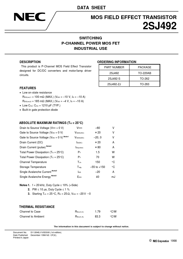
This product is P-Channel MOS Field Effect Transistor designed for DC/DC converters and motor/lamp driver circuits.| Part No. | 2SJ492 |
|---|---|
| Datasheet | 2SJ492 Download |
| Manufacturer |  NEC |
| Description | P-Channel MOSFET |
| Buy | Stock & Price |
DESCRIPTION
FEATURES
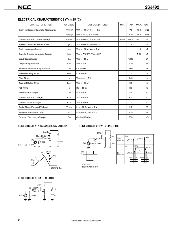
● Low on-state resistance RDS(on)1 = 100 mΩ (MAX.) (VGS = –10 V, ID = –10 A) RDS(on)2 = 185 mΩ (MAX.) (VGS = –4 V, ID = –10 A)● Low Ciss: Ciss = 1210 pF (TYP.)
● Built-in gate protection diode
ABSOLUTE MAXIMUM RATINGS
(TA = 25°C) Drain to Source Voltage (VGS = 0 V) Gate to Source Voltage (VDS = 0 V) Gate to Source Voltage (VDS = 0 V) Drain Current (DC) Drain Current (pulse) Note2 Note1 VDSS VGSS(AC) VGSS(DC) ID(DC) ID(pulse) PT PT Tch Tstg –60 # 20 V V V A A W W °C °C A mJ –20, 0 # 20 # 80 Total Power Dissipation (TA = 25°C) Total Power Dissipation (TC = 25°C) Channel Temperature Storage Temperature Single Avalanche Current Single Avalanche Energy Note3 Note3 1.5 70 150 –55 to +150 –20 40 IAS EAS Notes 1. f = 20 kHz, Duty Cycle ≤ 10% (+Side) 2. PW ≤ 10 µs, Duty Cycle ≤ 1 % 3. Starting Tch = 25 °C, RA = 25 Ω, VGS = –20 V ¡ 0 THERMAL RESISTANCE Channel to Case Channel to Ambient Rth(ch-C) Rth(ch-A) 1.79 83.3 °C/W °C/W The information in this document is subject to change without notice.