2SK2409
2SK2409 is SWITCHING N-CHANNEL POWER MOSFET manufactured by NEC.
DESCRIPTION
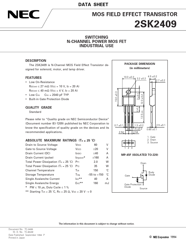
The 2SK2409 is N-Channel MOS Field Effect Transistor designed for solenoid, motor, and lamp driver. PACKAGE DIMENSION (in millimeters)
10.0 ±0.3 4.5 ±0.2 3.2 ±0.2 2.7 ±0.2
FEATURES
- Low On-Resistance
RDS(on) ≤ 27 mΩ (VGS = 10 V, ID = 20 A)
15.0 ±0.3
RDS(on) ≤ 40 mΩ (VGS = 4 V, ID = 20 A)
QUALITY GRADE
Standard Please refer to “Quality grade on NEC Semiconductor Device” (Document number IEI-1209) published by NEC Corporation to know the specification of quality grade on the devices and its remended applications.
2.54 0.7 ±0.1
4 ±0.2
13.5 MIN.
12.0 ±0.2
- Low Ciss Ciss = 2040 p F TYP.
- Built-in Gate Protection Diode
3 ±0.1
1.3 ±0.2 1.5 ±0.2 2.54
2.5 ±0.1 0.65 ±0.1 1. Gate 2. Drain 3. Source
ABSOLUTE MAXIMUM RATINGS (Ta = 25 ˚C)
Drain to Source Voltage Gate to Source Voltage Drain Current (DC) Drain Current (pulse) VDSS VGSS ID(DC) ID(pulse)- 60 ± 20 ± 40 ± 160 2.0 35 150 40 160 V V A A W W ˚C
Gate Drain 1 2 3
MP-45F (ISOLATED TO-220)
Total Power Dissipation (Ta = 25 ˚C) PT1 Total Power Dissipation (Tc = 25 ˚C) PT2 Channel Temperature Storage Temperature Single Avalanche Current Single Avalanche Energy
- PW ≤ 10 µs, Duty Cycle ≤ 1 % Tch Tstg IAS-
- EAS-
- - 55 to +150 ˚C A m J
Body Diode
Gate Protection Diode Source
- - Starting Tch = 25 ˚C, RG = 25 Ω, VGS = 20 V → 0
The information in this document is subject to change without notice. Document No. TC-2489 (O. D. No. TC-8028) Date Published September 1994 P Printed in Japan
©
ELECTRICAL CHARACTERISTICS (Ta = 25 ˚C)
CHARACTERISTIC Drain to Source On-State Resistance Drain to Source On-State Resistance Gate to Source Cutoff Voltage Forward Transfer Admittance Drain Cutoff Current Gate to Source Leakage Current Input Capacitance Output Capacitance Reverse Transfer Capacitance Turn-On Delay Time Rise Time Turn-Off Delay Time Fall Time Total Gate Charge Gate to Source Charge Gate to Drain Charge Body Diode Forward Voltage Reverse Recovery Time Reverse Recovery Charge SYMBOL...