UPA1725
UPA1725 is N-Channel Power MOSFET manufactured by NEC.
DATA SHEET
MOS FIELD EFFECT TRANSISTOR
µ PA1725
SWITCHING N-CHANNEL POWER MOS FET INDUSTRIAL USE
DESCRIPTION
This µPA1725 is N-Channel MOS Field Effect Transistor designed for power management applications of notebook puters and so on.
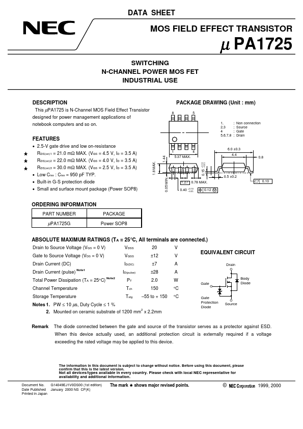
PACKAGE DRAWING (Unit : mm)
5 1, 2,3 4 5,6,7,8 ; ; ; ; Non connection Source Gate Drain
Features
- 2.5-V gate drive and low on-resistance
1.8 MAX.
- Built-in G-S protection diode
- Small and surface mount package (Power SOP8)
0.05 MIN.
- Low Ciss : Ciss = 950 p F TYP.
- RDS(on)3 = 30.0 mΩ MAX. (VGS = 2.5 V, ID = 3.5 A)
+0.10
- 0.05
- -
RDS(on)1 = 21.0 mΩ MAX. (VGS = 4.5 V, ID = 3.5 A) RDS(on)2 = 22.0 mΩ MAX. (VGS = 4.0 V, ID = 3.5 A)
1 5.37 MAX.
6.0 ±0.3 4.4 0.8
0.5 ±0.2 0.10
1.27 0.78 MAX. 0.40
+0.10
- 0.05
0.12 M
ORDERING INFORMATION
PART NUMBER PACKAGE Power...