

Datasheet Summary
DATA SHEET
MOS INTEGRATED CIRCUIT
µPD16326A
32-BIT FLUORESCENT DISPLAY TUBE DRIVER
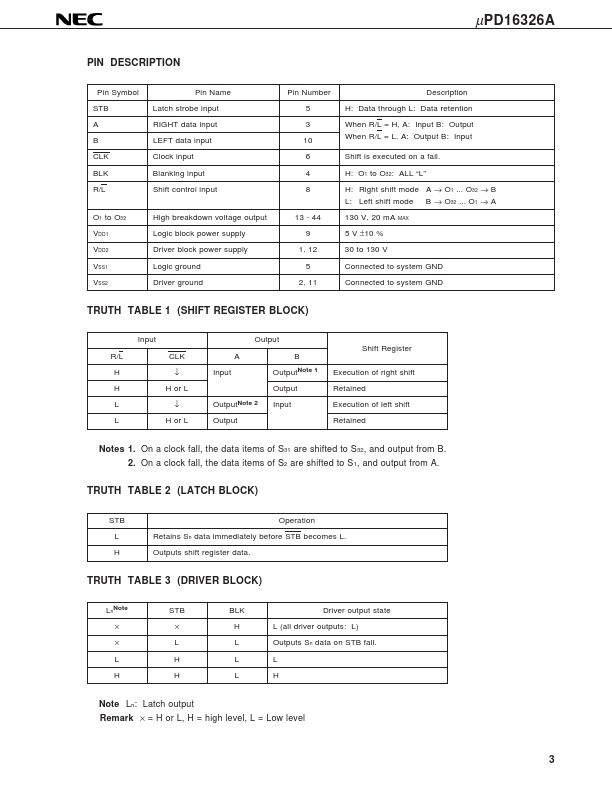
The µPD16326A is a fluorescent display tube driver using a high breakdown voltage CMOS process. It consists of 32-bit bidirectional shift registers, a latch circuit, and a high breakdown voltage CMOS driver block. The logic block operates on a 5 V power supply designed to be connected directly to a microcontroller (CMOS level input). The driver block has a 150 V and 20 mA high breakdown voltage output, and both the logic block and driver block consist of CMOS, allowing operation with low power consumption.
Features
- High breakdown voltage CMOS structure
- High breakdown voltage, high current output (150...