Datasheet Summary
DATA SHEET
MOS INTEGRATED CIRCUIT
µPD44165084, 44165184, 44165364
18M-BIT QDRTMII SRAM 4-WORD BURST OPERATION
Description
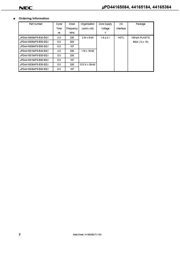
The µPD44165084 is a 2,097,152-word by 8-bit, the µPD44165184 is a 1,048,576-word by 18-bit and the
µPD44165364 is a 524,288-word by 36-bit synchronous quad data rate static RAM fabricated with advanced CMOS technology using full CMOS six-transistor memory cell. The µPD44165084, µPD44165184 and µPD44165364 integrates unique synchronous peripheral circuitry and a burst counter. All input registers controlled by an input clock pair (K and /K) are latched on the positive edge of K and /K. These products are suitable for application which require synchronous operation,...