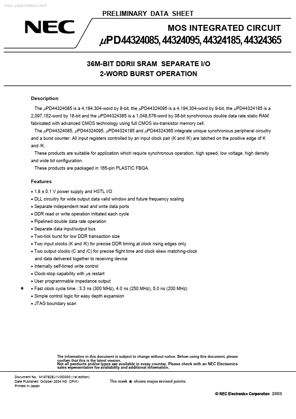
UPD44324365 Overview
Key Specifications
Package: FBGA
Pins: 165
Operating Voltage: 1.8 V
Max Voltage (typical range): 1.9 V
Description
The µPD44324085 is a 4,194,304-word by 8-bit, the µPD44324095 is a 4,194,304-word by 9-bit, the µPD44324185 is a 2,097,152-word by 18-bit and the µPD44324365 is a 1,048,576-word by 36-bit synchronous double data rate static RAM fabricated with advanced CMOS technology using full CMOS six-transistor memory cell. The µPD44324085, µPD44324095, µPD44324185 and µPD44324365 integrate unique synchronous peripheral circuitry and a burst counter.
Key Features
- 1.8 ± 0.1 V power supply and HSTL I/O
- DLL circuitry for wide output data valid window and future frequency scaling
- Separate independent read and write data ports
- DDR read or write operation initiated each cycle
- Pipelined double data rate operation
