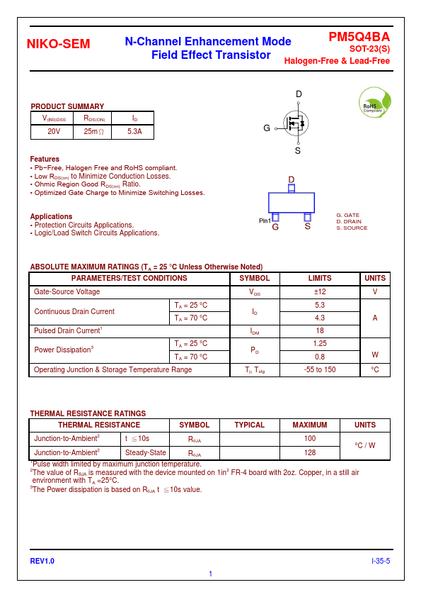
Datasheet4U Logo Datasheet4U.com

PM5Q4BA - N-Channel Field Effect Transistor

Download the PM5Q4BA datasheet PDF. This datasheet also covers the PM5Q4BA-NIKO variant, as both devices belong to the same n-channel field effect transistor family and are provided as variant models within a single manufacturer datasheet.

Key Features

  • Pb.
  • Free, Halogen Free and RoHS compliant.
  • Low RDS(on) to Minimize Conduction Losses.
  • Ohmic Region Good RDS(on) Ratio.
  • Optimized Gate Charge to Minimize Switching Losses.

📥 Download Datasheet

Note: The manufacturer provides a single datasheet file (PM5Q4BA-NIKO-SEM.pdf) that lists specifications for multiple related part numbers.

Datasheet Details

Part number PM5Q4BA
Manufacturer NIKO-SEM
File Size 192.03 KB
Description N-Channel Field Effect Transistor
Datasheet download datasheet PM5Q4BA Datasheet

Full PDF Text Transcription (Reference)

The following content is an automatically extracted verbatim text from the original manufacturer datasheet and is provided for reference purposes only.

View original datasheet text
NIKO-SEM N-Channel Enhancement Mode PM5Q4BA Field Effect Transistor SOT-23(S) Halogen-Free & Lead-Free PRODUCT SUMMARY V(BR)DSS RDS(ON) 20V 25mΩ ID 5.3A Features • Pb−Free, Halogen Free and RoHS compliant. • Low RDS(on) to Minimize Conduction Losses. • Ohmic Region Good RDS(on) Ratio. • Optimized Gate Charge to Minimize Switching Losses. Applications • Protection Circuits Applications. • Logic/Load Switch Circuits Applications. D G S G. GATE D. DRAIN S. SOURCE ABSOLUTE MAXIMUM RATINGS (TA = 25 °C Unless Otherwise Noted) PARAMETERS/TEST CONDITIONS SYMBOL Gate-Source Voltage Continuous Drain Current Pulsed Drain Current1 TA = 25 °C TA = 70 °C Power Dissipation3 TA = 25 °C TA = 70 °C Operating Junction & Storage Temperature Range VGS ID IDM PD Tj, Tstg LIMITS ±12 5.3 4.