Datasheet Summary
..
Low-power dual Schmitt trigger
Rev. 02
- 10 January 2008 Product data sheet
1. General description
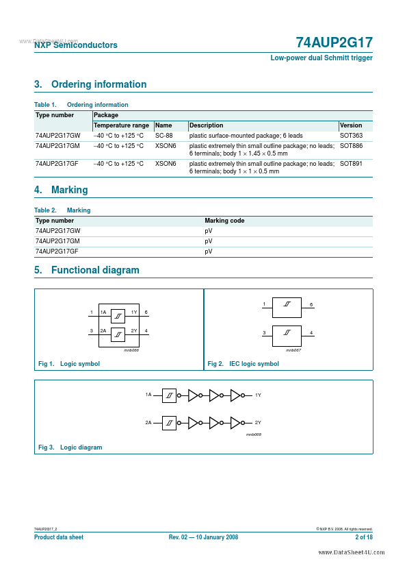
The 74AUP2G17 is a high-performance, low-power, low-voltage, Si-gate CMOS device, superior to most advanced CMOS patible TTL families. This device ensures a very low static and dynamic power consumption across the entire VCC range from 0.8 V to 3.6 V. This device is fully specified for partial power-down applications using IOFF. The IOFF circuitry disables the output, preventing the damaging backflow current through the device when it is powered down. The 74AUP2G17 provides two Schmitt trigger buffers. It is capable of transforming slowly changing input...