Datasheet Summary
Low-power dual Schmitt trigger
Rev. 9
- 31 January 2022
Product data sheet
1. General description
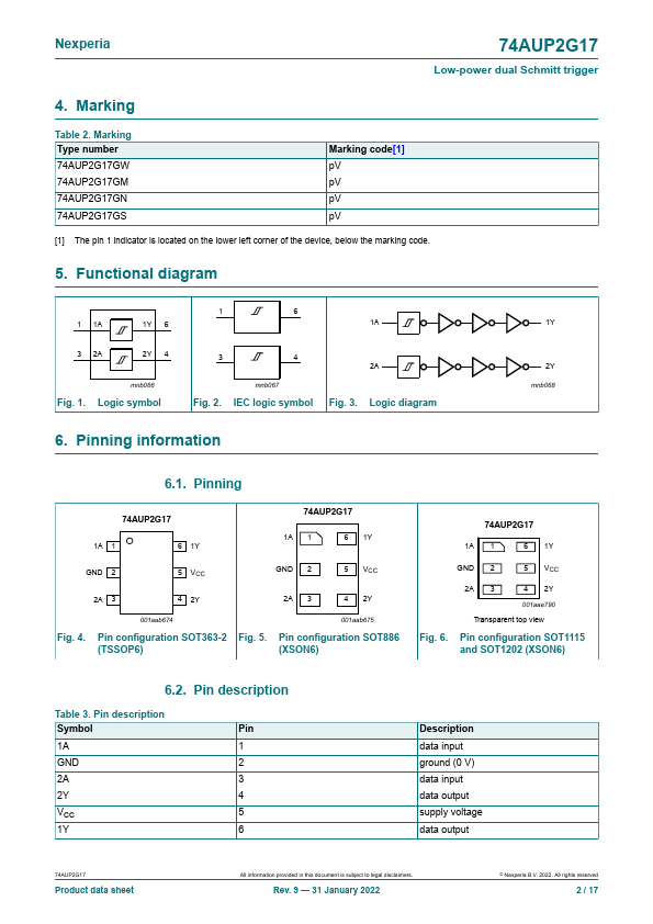
The 74AUP2G17 is a dual buffer with Schmitt-trigger inputs. This device ensures very low static and dynamic power consumption across the entire VCC range from 0.8 V to 3.6 V. This device is fully specified for partial power down applications using IOFF. The IOFF circuitry disables the output, preventing the potentially damaging backflow current through the device when it is powered down.
2. Features and benefits
- Wide supply voltage range from 0.8 V to 3.6 V
- CMOS low power dissipation
- High noise immunity
- Overvoltage tolerant inputs to 3.6 V
- Low noise overshoot and...