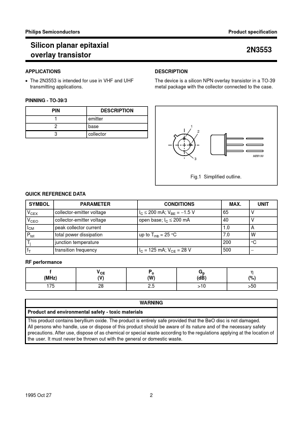
APPLICATIONS
● PINNING - TO-39/3 PIN 1 2 3 base collector handbook, halfpage 2N3553 DESCRIPTION
The device is a silicon NPN overlay transistor in a TO-39 metal package with the collector connected to the case. DESCRIPTION
emitter 1 2 MBB199 3 Fig.1 Simplified outline. QUICK REFERENCE DATA SYMBOL VCEX VCEO ICM Ptot Tj fT PARAMETER collector-emitter voltage collector-emitter voltage peak collector current total power dissipation junction temperature transition frequency IC = 125 mA; VCE = 28 V up to Tmb = 25 °C CONDITIONS IC ≤ 200 mA; VBE = −1.5 V open base; IC ≤ 200 mA 65 40 1.0 7.0 200 500 MAX. V V A W °C − UNIT RF performance f (MHz) 175 VCE (V) 28 Po (W) 2.5 Gp (dB) >10 η (%) >50 WARNING Product and environmental safety - toxic materials This product contains beryllium oxide. The product is entirely safe provided that the BeO disc is not damaged. All persons who handle, use or dispose of this product should be aware of its nature and of the necessary safety precautions. After use, dispose of as chemical or special waste according to the regulations applying at the location of the user. NXP Semiconductors