74LVT2952 Description
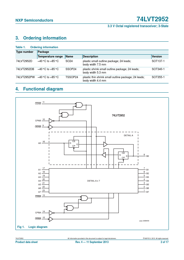
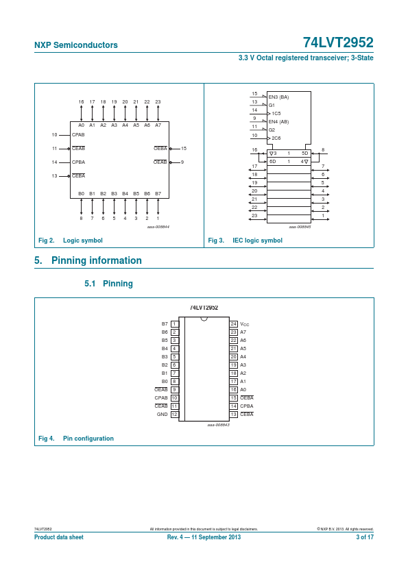
The 74LVT2952 is a high-performance BiCMOS product designed for VCC operation at 3.3 V. This device bines low static and dynamic power dissipation with high speed and high output drive. The 74LVT2952 device is an 8-bit registered transceiver.
74LVT2952 Key Features
- 8-bit registered transceiver
- Independent registers for A and B buses
- Input and output interface capability to systems at 5 V supply
- TTL input and output switching levels
- Output capability: +64 mA/32 mA
- Latch-up protection exceeds 500 mA per JESD78 class II level A
- ESD protection
- HBM JESD22-A114E exceeds 2000 V
- MM JESD22-A115-A exceeds 200 V
- Bus-hold data inputs eliminate the need for external pull-up resistors for unused inputs