NXP Semiconductors BFR53
NPN 2 GHz wideband transistor
| Part No. | BFR53 |
|---|---|
| Datasheet | BFR53 Download |
| Manufacturer |  NXP Semiconductors |
| Description | NPN 2 GHz wideband transistor |
| Buy | Stock & Price |
FEATURES
● Very low intermodulation distortion● Very high power gain.
APPLICATIONS
● Thick and thin-film circuits.DESCRIPTION
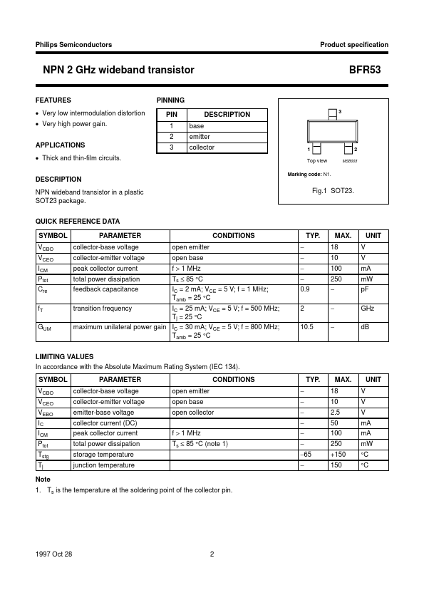
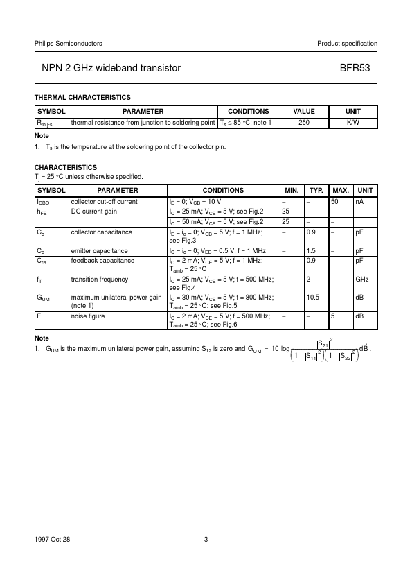
NPN wideband transistor in a plastic SOT23 package. QUICK REFERENCE DATA SYMBOL VCBO VCEO ICM Ptot Cre fT GUM PARAMETER collector-base voltage collector-emitter voltage peak collector current total power dissipation feedback capacitance transition frequency open emitter open base f > 1 MHz Ts ≤ 85 °C IC = 2 mA; VCE = 5 V; f = 1 MHz; Tamb = 25 °C IC = 25 mA; VCE = 5 V; f = 500 MHz; Tj = 25 °C CONDITIONS − − − − 0.9 2 10.5 TYP. PINNING PIN 1 2 3 base emitter collector 1 Top view Marking code: N1. BFR53DESCRIPTION
fpage 3 2 MSB003 Fig.1 SOT23. MAX. 18 10 100 250 − − − V V UNIT mA mW pF GHz dB maximum unilateral power gain IC = 30 mA; VCE = 5 V; f = 800 MHz; Tamb = 25 °C LIMITING VALUES In accordance with the Absolute Maximum Rating System (IEC 134). SYMBOL VCBO VCEO VEBO IC ICM Ptot Tstg Tj Note 1. Ts is the temperature at the soldering point of the collector pin.