BUK112-50GL
BUK112-50GL is Power MOSFET manufactured by NXP Semiconductors.
DESCRIPTION
Monolithic temperature and overload protected logic level power MOSFET in a 5 pin plastic envelope, intended as a low side switch for automotive applications.
QUICK REFERENCE DATA
SYMBOL VDS ID Tj RDS(ON) SYMBOL VPS PARAMETER Continuous drain source voltage Continuous drain current Continuous junction temperature Drain-source on-state resistance PARAMETER Protection supply voltage MAX. 50 12 150 93 NOM. 5 UNIT V A ˚C mΩ UNIT V
FEATURES
Vertical power DMOS output stage Low on-state resistance Low operating supply current Overtemperature protection Overload protection against short circuit load with drain current limiting Latched overload protection reset by protection supply Protection circuit condition indicated by flag pin Off-state detection of open circuit load indicated by flag pin 5 V logic patible input level Integral input resistors. ESD protection on all pins Over voltage clamping
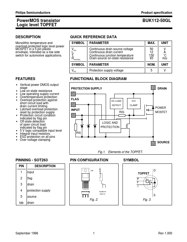
FUNCTIONAL BLOCK DIAGRAM
PROTECTION SUPPLY DRAIN
FLAG
OC LOAD DETECT
O/V CLAMP
INPUT
POWER RIG MOSFET
LOGIC AND PROTECTION RIS SOURCE
Fig.1. Elements of the TOPFET.
PINNING
- SOT263
PIN 1 2 3 4 5 tab input flag drain protection supply source DESCRIPTION
PIN CONFIGURATION tab
SYMBOL
D TOPFET P F I
1 2345 leadform 263-01
Fig. 2. drain
Fig. 3.
September 1996
Rev 1.000
Philips Semiconductors
Product specification
Power MOS transistor Logic level TOPFET
LIMITING VALUES
Limiting values in accordance with the Absolute Maximum Rating System (IEC 134) SYMBOL VDS ID II IF IP Ptot Tstg Tj Tsold PARAMETER Continuous voltage Drain source voltage1 Continuous currents Drain current Input current Flag current Protection supply current Thermal Total power dissipation Storage temperature Junction temperature2 Lead temperature Tmb = 25 ˚C continuous during soldering -55 VPS = 5 V; Tmb = 25 ˚C VPS = 0 V; Tmb = 94 ˚C -5 -5 -5 VIS = 0 V CONDITIONS MIN.
MAX. 50 self limited 12 5 5 5 52 175 150 260
UNIT V A A m A m A m A W ˚C ˚C ˚C
ESD...