BUK9609-55A
BUK9609-55A is (BUK9x09-55A) TrenchMOS logic level FET manufactured by NXP Semiconductors.
- Part of the BUK9509-55A comparator family.
- Part of the BUK9509-55A comparator family.
Description
N-channel enhancement mode field-effect power transistor in a plastic package using Trench MOS™ technology, featuring very low on-state resistance. Product availability: BUK9509-55A in SOT78 (TO-220AB) BUK9609-55A in SOT404 (D2-PAK).
2. Features s s s s Trench MOS™ technology Q101 pliant 175 °C rated Logic level patible.
3. Applications s Automotive and general purpose power switching: x 12 V and 24 V loads x Motors, lamps and solenoids.
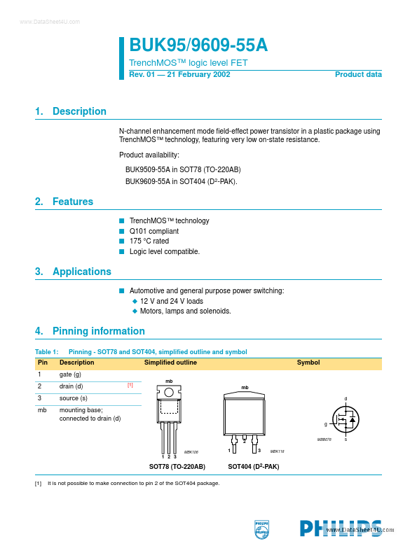
4. Pinning information
Table 1: Pin 1 2 3 mb Pinning
- SOT78 and SOT404, simplified outline and symbol Description gate (g) drain (d) source (s) mounting base; connected to drain (d) g s
[1]
Simplified outline mb mb
Symbol d
MBK106
MBB076
MBK116
1 2 3
SOT78 (TO-220AB)
[1] It is not possible to make connection to pin 2 of the SOT404 package.
SOT404 (D2-PAK)
..
Philips Semiconductors
BUK95/9609-55A
Trench MOS™ logic level FET
5. Quick reference data
Table 2: VDS ID Ptot Tj RDSon Quick reference data Conditions Tmb = 25 °C; VGS = 5 V Tmb = 25 °C Tj = 25 °C; VGS = 5 V; ID = 25 A Tj = 25 °C; VGS = 4.5 V; ID = 25 A Tj = 25 °C; VGS = 10 V; ID = 25 A Typ 7.6 6.4 Max 55 108 211 175 9 10 8 Unit V A W °C mΩ mΩ mΩ drain-source voltage (DC) drain current (DC) total power dissipation junction temperature drain-source on-state resistance Symbol Parameter
6. Limiting values
Table 3: Limiting values In accordance with the Absolute Maximum Rating System (IEC 60134). Symbol Parameter VDS VDGR VGS ID drain-source voltage (DC) drain-gate voltage (DC) gate-source voltage (DC) drain current (DC) Tmb = 25 °C; VGS = 5 V; Figure 2 and 3 Tmb = 100 °C; VGS = 5 V; Figure 2 IDM Ptot Tstg Tj IDR IDRM peak drain current total power dissipation storage temperature junction temperature reverse drain current (DC) peak reverse drain current Tmb = 25 °C Tmb = 25 °C; pulsed; tp ≤ 10 µs unclamped inductive load; ID = 75 A; VDS ≤ 55 V; VGS = 5 V; RGS = 50 Ω; starting Tmb = 25 °C
[1] [2] [1] [2] [2]
Conditions RGS = 20 kΩ
Min
- 55
- 55
-...