NXP Semiconductors GTL16612
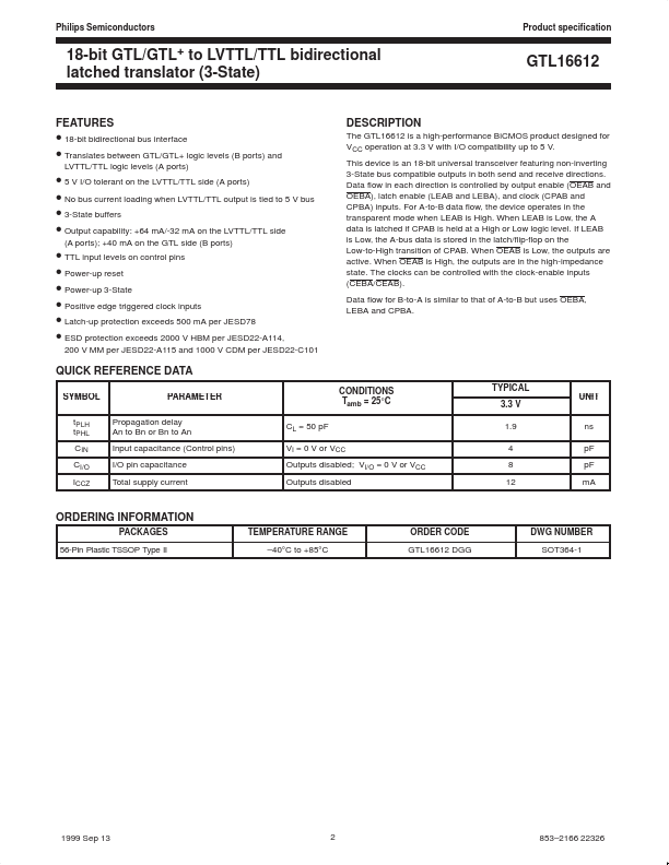
The GTL16612 is a high-performance BiCMOS product designed for VCC operation at 3.3 V with I/O compatibility up to 5 V. This device is an 18-bit universal transceiver featuring non-inverting 3-State bus compatible outputs in both send and receive directions. For A-to-B data flow, the device operates in the transparent mode when LEAB is High.| Part No. | GTL16612 |
|---|---|
| Datasheet | GTL16612 Download |
| Manufacturer |  NXP Semiconductors |
| Description | 18-bit GTL/GTL to LVTTL/TTL bidirectional latched translator 3-State |
| Buy | Stock & Price |

FEATURES
● 18-bit bidirectional bus interface● Translates between GTL/GTL+ logic levels (B ports) and
● 5 V I/O tolerant on the LVTTL/TTL side (A ports)
● No bus current loading when LVTTL/TTL output is tied to 5 V bus
● 3-State buffers
● Output capability: +64 mA/-32 mA on the LVTTL/TTL side
● TTL input levels on control pins
● Power-up reset
● Power-up 3-State
● Positive edge triggered clock inputs
● Latch-up protection exceeds 500 mA per JESD78
● ESD protection exceeds 2000 V HBM per JESD22-A114, 200 V MM per JESD22-A115 and 1000 V CDM per JESD22-C101 (A ports); +40 mA on the GTL side (B ports) LVTTL/TTL logic levels (A ports)
DESCRIPTION
Data flow in each direction is controlled by output enable (OEAB and OEBA), latch enable (LEAB and LEBA), and clock (CPAB and CPBA) inputs. When LEAB is Low, the A data is latched if CPAB is held at a High or Low logic level. If LEAB is Low, the A-bus data is stored in the latch/flip-flop on the Low-to-High transition of CPAB. When OEAB is Low, the outputs are active.