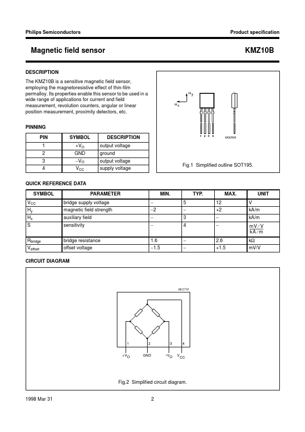
DESCRIPTION
PINNING PIN 1 2 3 4 SYMBOL +VO GND −VO VCC DESCRIPTION
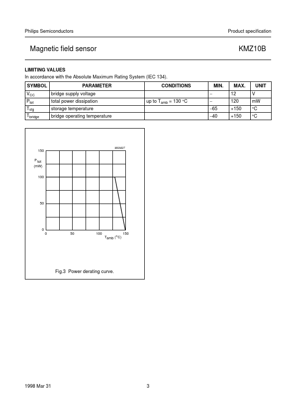
output voltage ground output voltage supply voltage 1 2 3 4 MGD806 KMZ10B handbook, halfpage Hy Hx Fig.1 Simplified outline SOT195. QUICK REFERENCE DATA SYMBOL VCC Hy Hx S Rbridge Voffset PARAMETER bridge supply voltage magnetic field strength auxiliary field sensitivity bridge resistance offset voltage − −2 − − 1.6 −1.5 MIN. 5 − 3 4 − − TYP. 12 +2 − − 2.6 +1.5 MAX. V kA/m kA/m mV ⁄ V ---------------kA ⁄ m kΩ mV/V UNIT CIRCUIT DIAGRAM handbook, full pagewidth MLC716 1 +VO 2 GND 3 –VO 4 VCC Fig.2 Simplified circuit diagram. 1998 Mar 31 2 Philips Semiconductors Product specification Magnetic field sensor LIMITING VALUES In accordance with the Absolute Maximum Rating System (IEC 134). SYMBOL VCC Ptot Tstg Tbridge PARAMETER bridge supply voltage total power dissipation storage temperature bridge operating temperature up to Tamb = 130 °C CONDITIONS − − −65 −40 MIN. KMZ10B MAX. 12 120 +150 +150 V UNIT mW °C °C handbook, halfpage 150 MSA927 P tot (mW) 100 50 0 0 50 100 Tamb (o C) 150 Fig.3 Power derating curve. NXP Semiconductors