MRF6V12500H
Features
- Characterized with Series Equivalent Large--Signal Impedance Parameters
- Internally Matched for Ease of Use
- Qualified up to a Maximum of 50 VDD Operation
- Integrated ESD Protection
- Greater Negative Gate--Source Voltage Range for Improved Class C
Operation
Document Number: MRF6V12500H Rev. 5, 7/2016
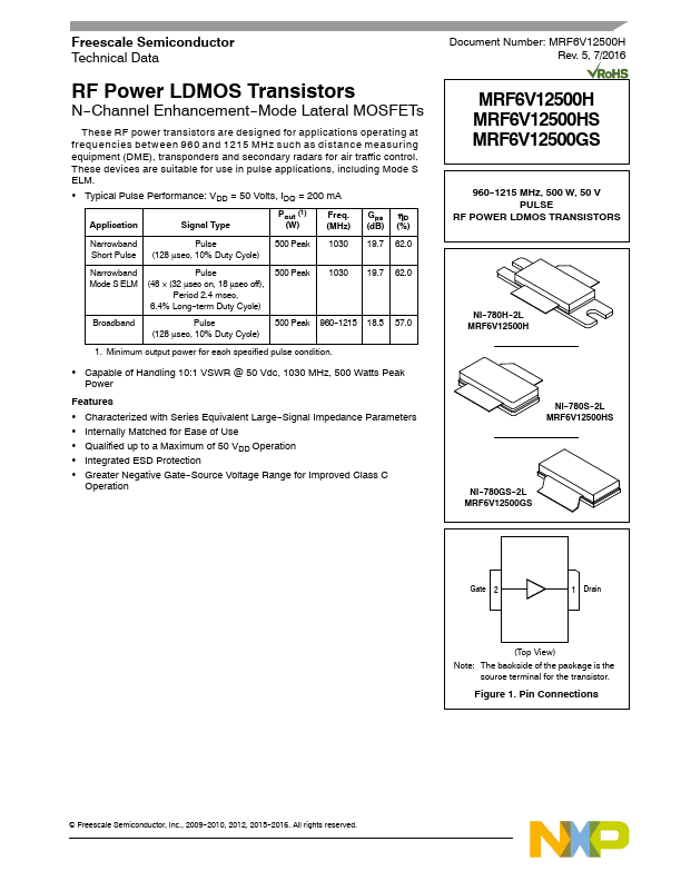
MRF6V12500H MRF6V12500HS MRF6V12500GS
960--1215 MHz, 500 W, 50 V PULSE
RF POWER LDMOS TRANSISTORS
NI--780H--2L MRF6V12500H
NI--780S--2L MRF6V12500HS
NI--780GS--2L MRF6V12500GS
Gate 2
1 Drain
(Top View) Note: The backside of the package is the source terminal for the transistor.
Figure 1. Pin Connections
Freescale Semiconductor, Inc., 2009--2010, 2012, 2015--2016. All rights reserved.
RF Device Data Freescale Semiconductor, Inc.
MRF6V12500H MRF6V12500HS MRF6V12500GS 1
Table 1. Maximum Ratings
Rating
Symbol
Value
Unit
Drain--Source Voltage Gate--Source Voltage Storage Temperature Range Case Operating Temperature Operating Junction Temperature (1,2)
Table 2....