CD4015BC
Overview
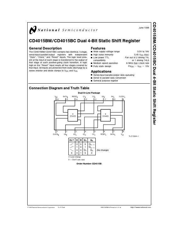
The CD4015BM CD4015BC contains two identical 4-stage serial-input parallel-output registers with independent ‘‘Data’’ ‘‘Clock ’’ and ‘‘Reset’’ inputs The logic level present at the input of each stage is transferred to the output of that stage at each positive-going clock transition A logic high on the ‘‘Reset’’ input resets all four stages covered by that input All inputs are protected from static discharge by a series resistor and diode clamps to VDD and VSS.