DM54L04
DM54L04 is Hex Inverting Gate manufactured by National Semiconductor.
DM54L04 Hex Inverting Gate
July 1989
DM54L04 Hex Inverting Gate
General Description
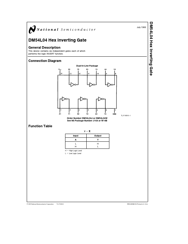
This device contains six independent gates each of which performs the logic INVERT function
Connection Diagram
Dual-In-Line Package
TL F 6616
- 1
Order Number DM54L04J or DM54L04W See NS Package Number J14A or W14B
Function Table
YeA Input A L H
H e High Logic Level L e Low Logic Level
Output Y H L
C1995 National Semiconductor Corporation
TL F 6616
RRD-B30M105 Printed in U S...